Recent Posts

Designing a keyboard from scratch - Part 4

52 minute read

Welcome to the 4th episode of this series of articles about designing a full keyboard from scratch. So far we’ve seen:

I’ll now cover:

  • production of manufacturing outputs
  • ordering the PCBs
  • selecting the correct components
  • assembling the PCB
  • creating the firmware
  • and finally testing the PCB

This is again a long episode that took quite long time to write, sorry for the wait. Feel free to leave a comment if you have any questions or find anything suspect :)

Getting manufacturing files

We need to export our PCB out of Kicad and send it to the factory. Hopefully, all the factories out there use a common file format that is called the Gerber format.

This file format is a vectorial format that describe precisely the layer traces and zones, silk screens, and sometimes where to drill holes (some manufacturer require Excellon format). This has become a kind of interchange standard for PCB factories. This is an old file format that was used to send numerical commands to Gerber plotters in the 70s. Since then the format has evolved and we’re dealing now with Extended Gerber files.

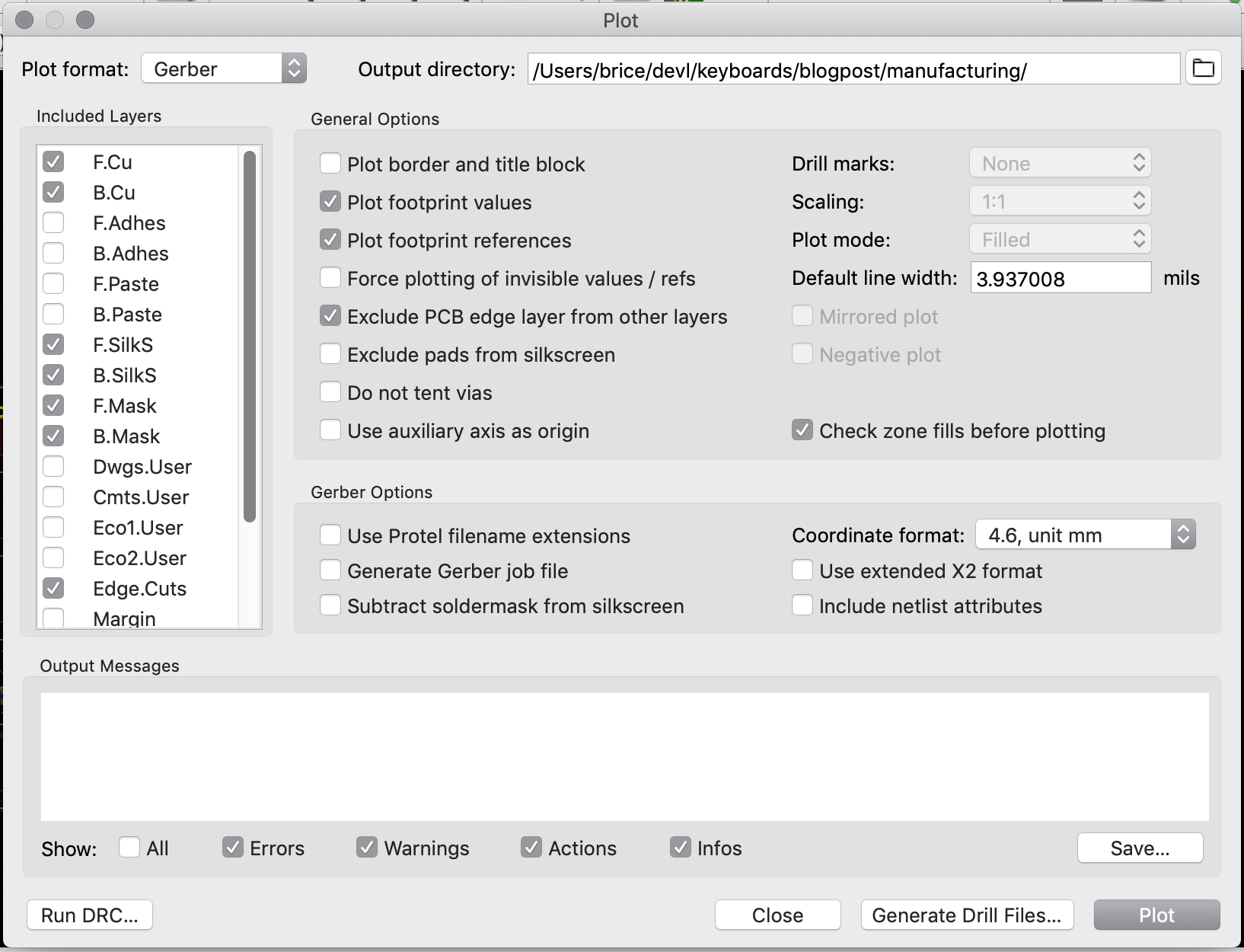
Back to my PCB, I can generate my set of Gerber files to be sent to the factory from pcbnew by going to File → Plot…. A new window opens where I can configure the output.

The options to set will depend on the manufacturer. Here’s a few manufacturer Kicad recommandations and settings:

Caution: different manufacturer have different tolerances and capabilities (for instance minimum track size, via size, board size, etc). Make sure you check with them if your PCB can be manufactured.

This time, I’m going to be using JLCPCB. Here’s the recommended setup for JLCPCB with Kicad 5.1:

Plot Gerber

For this project the following layers needs to be checked:

  • F.Cu
  • B.Cu
  • F.SilkS
  • B.SilkS
  • F.Mask
  • B.Mask
  • Edge.Cuts

The first two are for drawing the tracks and pads, the two next ones are the components reference and value indications (and the art), the two mask layers contains the zone where the copper layers will be seen (ie pads and holes), and finally the Edge.Cuts layer contains the board outline.

Make sure the chosen format is Gerber, then choose a sensible output folder (I like to put those files in a manufacturing subfolder of my PCB repository).

And additionnally those options need to be checked:

  • Check Zone fills before plotting - to make sure zones have been recomputed
  • Plot footprint values - because our switch footprints have the key name as values in the silkscreen
  • Plot footprint references - because all the components except the switches have a unique reference (that will help locate the component when soldering)
  • Exclude PCB Edge from other layers

When clicking on the Plot button, the files are generated (in the folder previously entered).

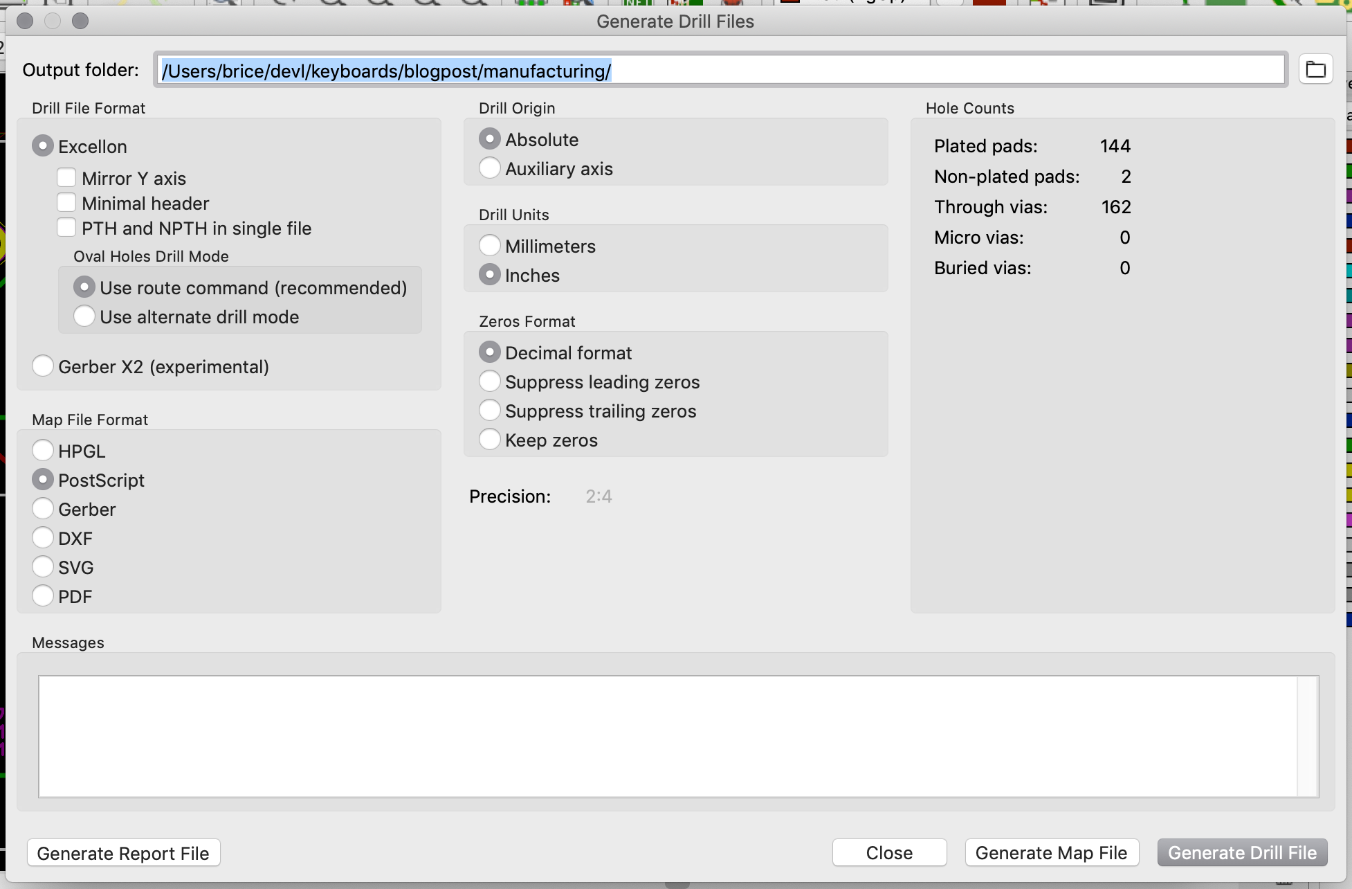
The next step is to generate the drill files, which contain the location where to drill holes (for both types of holes: mounting holes or for through-hole components, and for plated and non-plated holes). This can be done by clicking on the Generate Drill Files button next to the Plot button in the previous window:

Plot Gerber

The important options to check are:

  • Excellion
  • Use route command
  • Postscript

Generating the drill file is done by clicking on the Generate Drill File (oh that was unexpected :) ) This produces two new files in my manufacturing folder, one for the plated holes and the other ones for the non-plated holes. The manufacturing folder now contains:

  • aek67-B_Cu.gbr
  • aek67-B_Mask.gbr
  • aek67-B_SilkS.gbr
  • aek67-Edge_Cuts.gbr
  • aek67-F_Cu.gbr
  • aek67-F_Mask.gbr
  • aek67-F_SilkS.gbr
  • aek67-NPTH.drl
  • aek67-PTH.drl

Now zip everything (cd manufacturing ; zip -r pcb.zip * if you like the command-line). That’s what we’re going to upload to the manufacturer.

Manufacturing

If you’re interested in PCB manufacturing, you can watch this video of the JLCPCB factory, you’ll learn a ton of things about how PCB are made these days.

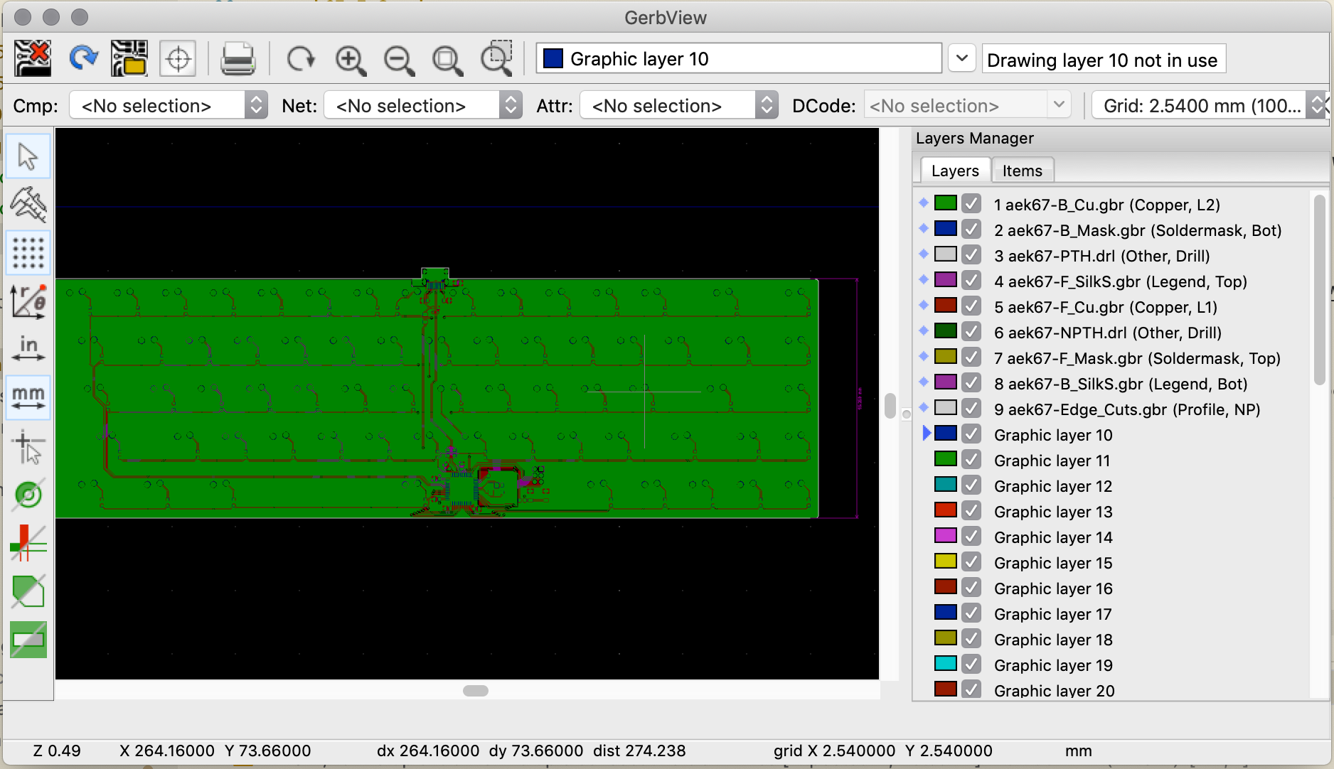
So, the process is to upload the Gerber and drill files to the factory. But first it’s best to make sure those files are correct. Kicad integrates a Gerber viewer to do that. It’s also possible to check with an online Gerber viewer like for instance Gerblook or PCBxprt.

The Kicad viewer can be launched from the Kicad project window with Tools → View Gerber Files. The next step is to load the gerber files in the viewer with the File → Open ZIP file and point it to the pcb.zip file of the previous chapter.

This gives this result:

Gerber Viewer

So, what to check in the viewer files?

  1. check that the files can be correctly opened
  2. check each layers independently
  3. for copper layers, check that the pads seems correct
  4. for soldermask layers, check that the soldermask doesn’t appear on pads
  5. for silkscreen layers, check that components’ references and values appear correctly, then check the silkscreen art and text if there are some.

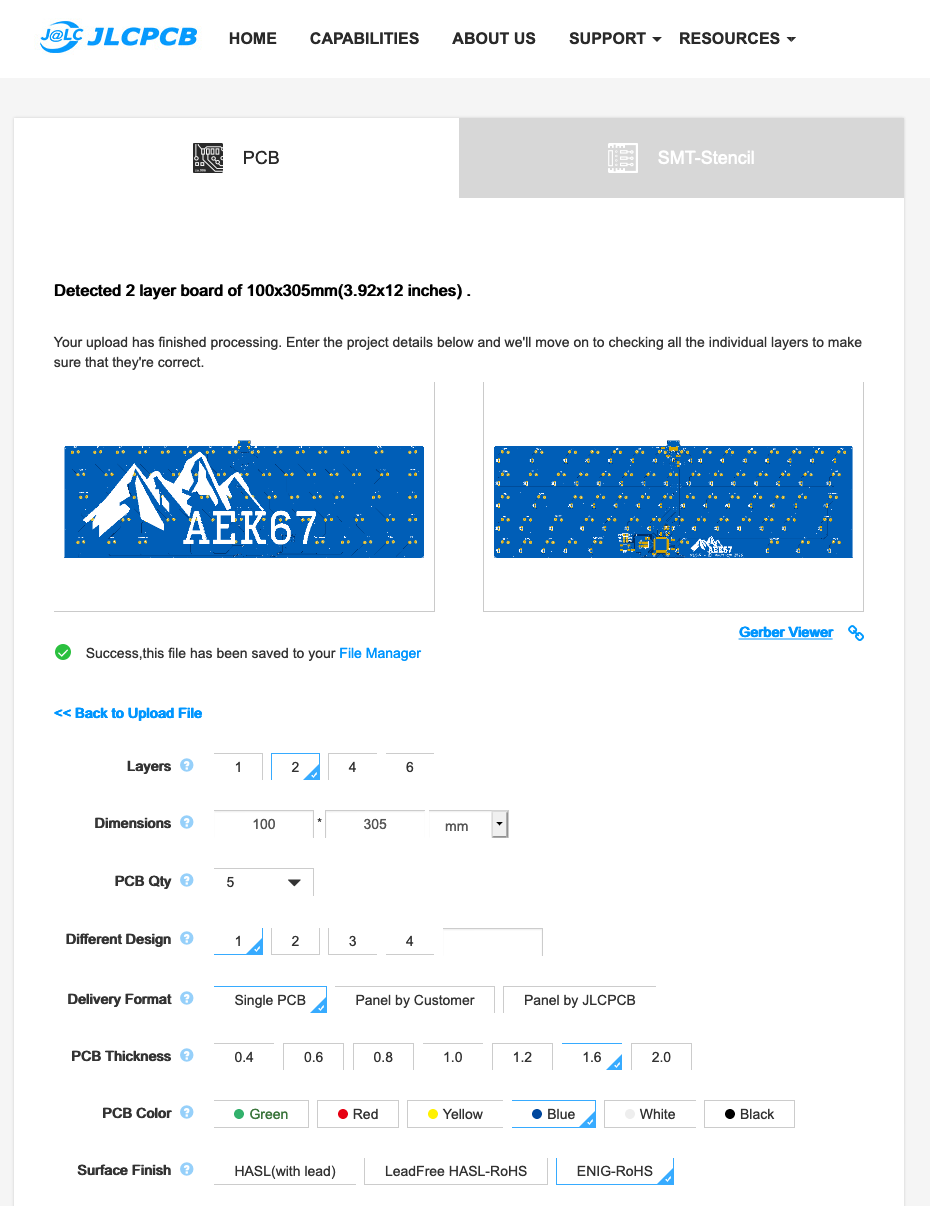
Once this basic verification has been done, it’s time to upload the zip file to the manufacturer website. Once the file is uploaded, the site will display the gerber file. Make sure to check again the layers, as this time it’s the manufacturer interpretation of the files. With JLCPCB the interface looks like this:

JLCPCB ordering

In this screenshot, I have omitted the price calculation and the bottom part (we’ll get to this one below). You can see the gerber view, and most manufacturer host an online gerber viewer to make sure the files are correctly loaded.

Immediately below, there’s the choice of number of layers and pcb dimensions. Those two numbers have been detected from the uploaded file. Make sure there’s the right number of layers (two in this case), and that the dimensions are correct. If not, check the gerber files or original Kicad files edge cutout.

The next set of options deals with the number of PCB and their panelisation:

JLCPCB ordering

Paneling is the process of grouping multiple PCB on the same manufacturing board. The manufacturer will group several PCB (from either the same customer or different customers) on larger PCB. You can have the option of grouping your PCB the way you want, depending on the number of different designs you uploaded. On my case, this is straightforward as there’s only one design that doesn’t need to be panelized. Even though, I’m going to build only one keyboard, the minimum order quantity is 5 pieces. But that’s not as bad as it seems, because that will leave me the freedom of failing the assembly of a few boards :)

The next set of options are the technical characteristics of the board:

JLCPCB ordering

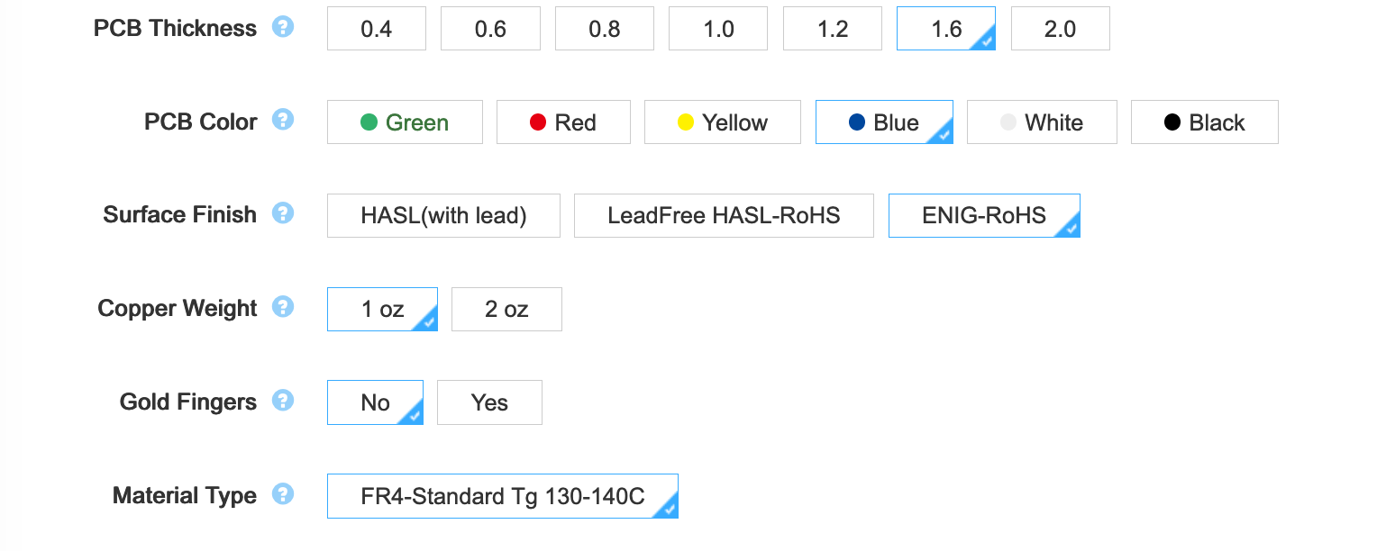
There we can change the thickness, color, finish, copper weight etc.

Those parameters are important so I need to explain what to choose. The PCB thickness represents the thickness of the FR4 fiber glass board sandwiched by the two copper layers which are later on etched to form the tracks. For a regular keyboard the standard is 1.6 mm. If you want to build a keyboard with more flex, you can opt for a 1.2 mm PCB. Note that in this case, it will not be possible to properly use PCB snap-in stabilizers (hopefully it won’t be an issue for screw-in stabilizers or plate stabilizers). Since this PCB is to be used in a regular keyboard, the default 1.6 mm is to be used.

The PCB color is a matter of preference of course. Just know that the final price is dependent on the chosen color. Most PCBs manufactured by JLCPCB are green, so this color is a lot cheaper (and take less lead/build time) than blue ones. Since the beginning of this series I was showing a blue soldermask so I decided to keep using a blue soldermask. I got a warning that it would mean two extra days of lead time.

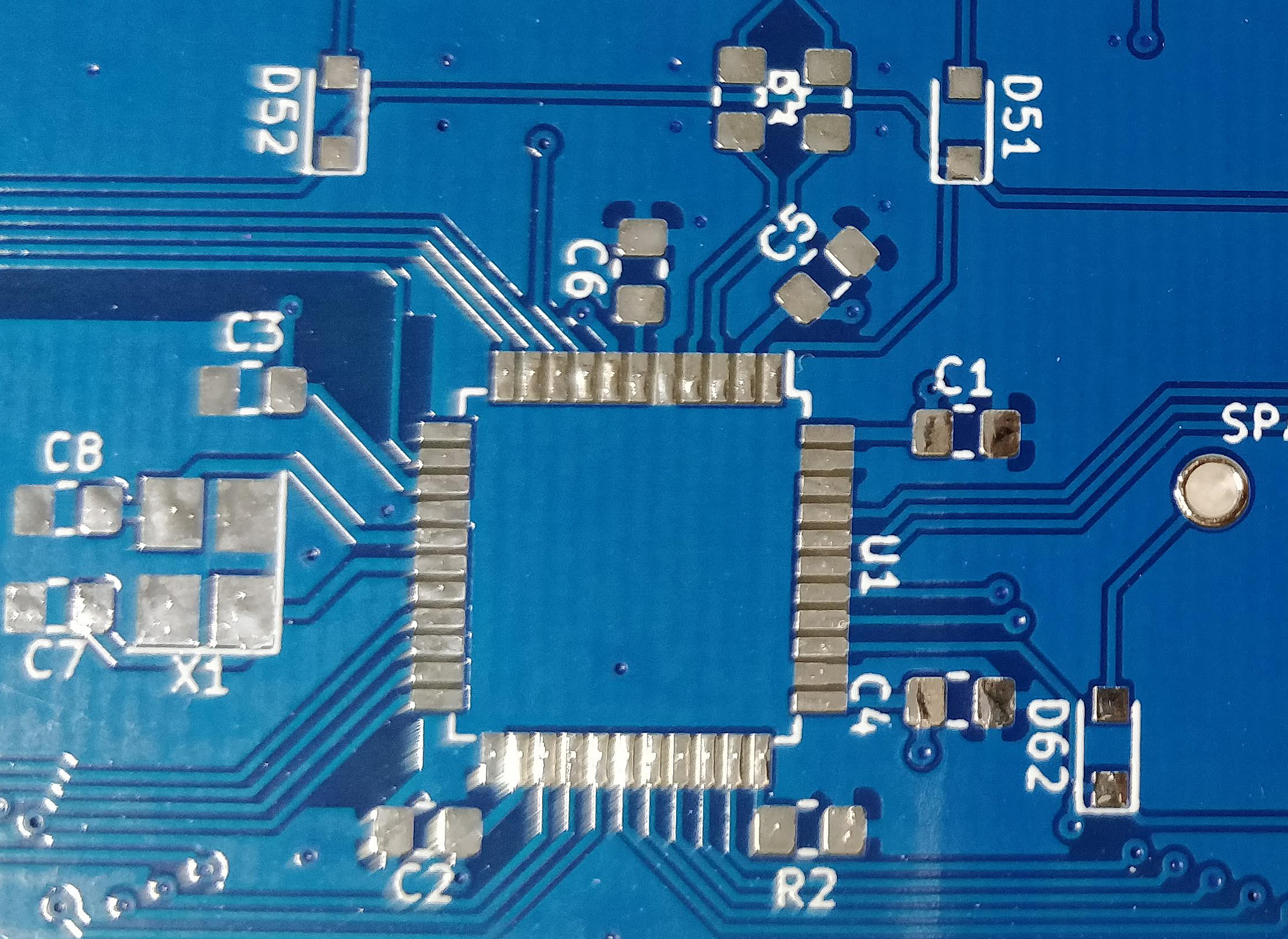
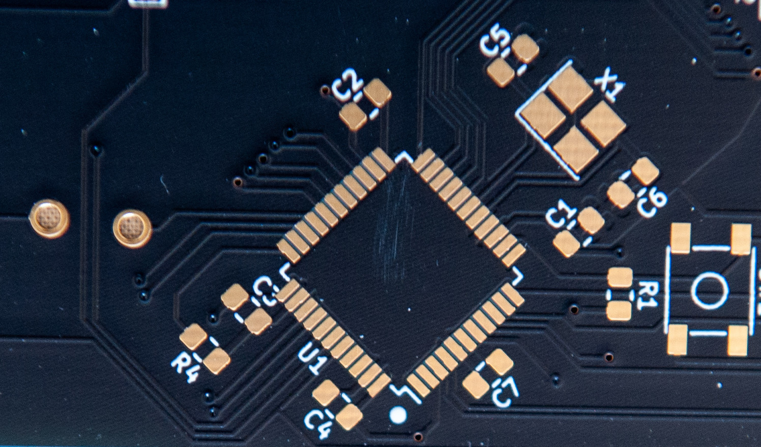
Surface finish is how the pads and through-holes are plated. There are three possibilities, HASL, lead-free HASL, and ENIG. Technically the two first ones are equivalent.

HASL ENIG

The pads’ copper will oxidize with time at the contact with air. Those solderable parts of the PCB must be protected by a surface treatment to prevent oxidation. The HASL (Hot Air Solder Leveling) and its lead-free variant consist in dropping a small amount of solder tin-alloy on all the visible copper parts. ENIG or Electroless Nickel Immersion Gold is a plating process consisting in plating the copper with a nickel alloy and then adding a very thin layer of gold on top of it (both operations are chemical operations where the board is dipped in special solutions). I did test both options, and I really favor ENIG over HASL (despite the price increase). I found that it is easier to solder SMD components on ENIG boards than on HASL ones (the solder seems to better wet and flow, also the surface is completely flat on ENIG boards so it’s easier to place components).

The copper weight is in fact a measure of the copper thickness on each layer. The default is 1 oz, which means a thickness of 35 µm. Using a thicker copper layer would change the trace thickness and thus their electrical characteristics (inductance, impedance and such). The default of 1 oz is fine for most use cases.

Next gold fingers. This isn’t needed for most PCB (especially keyboards). Gold fingers are visible connection traces on the edge of the PCB that are used to slot-in a daughter card in a connector.

Finally for 2-layers boards, JLCPCB doesn’t offer to choose a different board material than regular FR4.

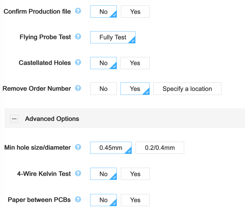
The next set of options are less important and some are straightforward:

JLCPCB ordering

I will just talk about castellation holes. Those are plated holes at the edge of the board. They will be cut in half in the process (if the option is selected). One of the use case is to join and solder two distinct pcb by the edge, using either solder joints or specialized connectors. This option is not needed for this project.

And finally the last option is the possibility to have the pcb separated by a piece of paper when packed. JLCPCB quality is reasonably good, but I had a few of my PCBs with partly scratched silkscreen or soldermask. It’s up to you to select or not this option (it increases the price because of the extra labor).

Before ordering, it is also possible to purchase assembly. In this case, all the components will be soldered at the factory (though they only support one face and only some specific parts, USB receptacles for instance are not available). If selected, you’ll need to provide the BOM and the parts position/orientation (Kicad can gnerate this placement file, but there are some recent Kicad versions generating files with bad parts orientations). Since this would spoil the fun of soldering SMD parts by hand, I won’t select it.

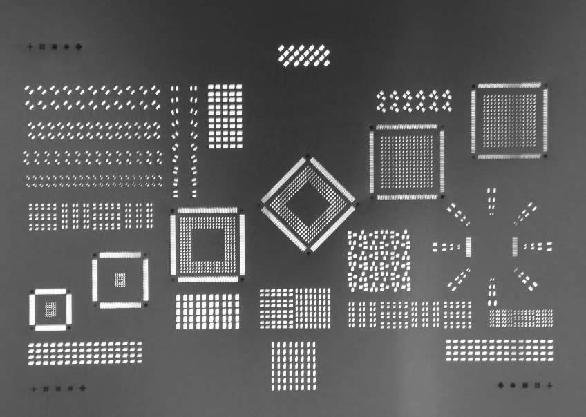
It’s also possible to order a stencil. A stencil is a metal sheet with apertures at the pads locations (imagine the soldermask but as a metal sheet), here’s an example:

SMT Stencil

When soldering with a reflow oven or an hot air gun (or even an electric cooking hot plate)), the stencil is used to apply solder paste on the pads. This technique is demonstrated in this video. I don’t need this option either, as I intend to hand solder with a soldering iron the SMD components.

The next step is to finalize the order, pay and wait. Depending on the options (mostly the soldermask color), it can take from a couple of days to more than a week for the PCBs to be manufactured. Shipping to EU takes between one or two weeks depending on the chosen carrier (and the pandemic status).

A PCB without any components is of no use. So while waiting for the boards to be manufactured and shipped to me, let’s order the components.

Selecting parts

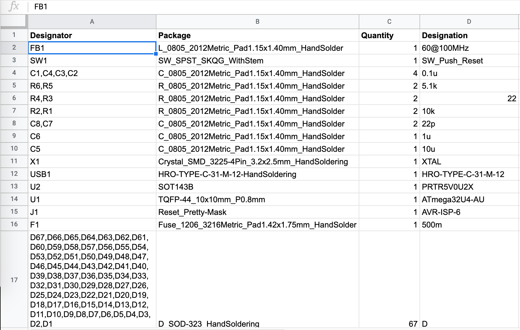
Kicad is able to generate a BOM list with the File → Fabrication Output → BOM File... This produces a CSV file. Note that it’s not a regular CSV where fields are separated by commas, instead they are using semicolon separators. This file can be loaded into a spreadsheet software. After cleaning it a bit (removing the switches and logos), it gives this kind of table:

Components

This will be of great help to know how many components I have to order to build one PCB (or the 5 ordered in the previous chapter).

So in a nutshell, for this keyboard, the following parts need to be sourced:

Designation Type Footprint Quantity
FB1 Ferrite Bead 0805 1
SW1 Reset switch SKQG 1
C1-C4 100nF Capacitor 0805 4
C5 10uF Capacitor 0805 1
C6 1uF Capacitor 0805 1
C7, C8 22pF Capacitor 0805 2
R1, R2 10kΩ Resistor 0805 2
R3, R4 22Ω Resistor 0805 2
R5, R6 5.1kΩ Resistor 0805 2
X1 16 MHz Crystal 3225 1
USB1 USB Connector HRO-TYPE-C-31-M-12 1
U2 PRTR5V0U2X SOT143B 1
U1 Atmega 32U4-AU TQFP-44 1
F1 PTC Fuse 1206 1
D1-D67 Diode SOD-123 67

First, let’s see where electronic parts can be bought. There are lots of possibilities. I don’t recommend sourcing from random stores on AliExpress, but instead ordering from professional vendors. You’ll be sure to get genuine parts (and not counterfeited components). Professional vendors will also store and ship correctly components in term of humidity and ESD protections.

I usually buy parts from the following vendors (because I’m based in the EU, I tend to favor European vendors):

  • LCSC, this is the JLCPCB sister company. China located, they ship everywhere. Most of the time you can purchase in small quantities (ie > 10). They occasionally run out of AtMega32U4. There’s a risk of customs taxes when shipping to Europe.
  • RS Components, ships from Europe (VAT included) with free shipping in France for week-end orders.
  • TME, based in Poland (VAT included), very fast shipping to European Countries
  • Mouser, they also ship from Europe for European customers.
  • Digikey, ships from the US (subject to customs taxes for Europeans)

I usually order from LCSC, TME and RS. With a predilection for TME lately. Almost all those vendors carry the same kind of components, sometimes even from the same manufacturers (for the most known ones like Murata, Vishay, etc). On LCSC, you’ll also find components made by smaller Chinese companies that can’t be found anywhere else.

All those vendors also provide components’ datasheets which is very useful to select the right part. For all components, I’ve added a table with links to the parts on LCSC, TME and Digikey.

Diodes

The diodes are the simplest component to select. A keyboard needs basic signal switching diodes, the most iconic one is the 1N4148. I selected the SOD-123 package reference 1N4148W-TP from MCC.

Reference LCSC TME Digikey
D1-D67 C77978 1N4148W-TP 1N4148WTPMSCT-ND

PTC Resettable Fuse

To select a PTC resettable fuse, one need to know its basic characteristics. USB is able to deliver at max 500 mA (because that’s what the 5.1 kΩ pull up resistors R5 and R6 says to the host), so ideally the fuse should trip for any current drawn above 500 mA. Based on this, I can select a part that has the 1206 SMD form factor and a reasonable voltage.

I selected the TECHFUSE nSMD025-24V on the LCSC site. It trips at 500mA, is resettable (ie once it triggers, it will stop conducting, but will become conducting again after the surge), and it can sustain up to 100A (which is large enough to absorb any electrical surge). This specific part is not available from the other vendors, but can be substituted by the Bell Fuse 0ZCJ0025AF2E (other manufacturer’s part can also match).

This component looks like this:

PTC Fuse

To summarize:

Reference LCSC TME Digikey
F1 C70069 0ZCJ0025AF2E 507-1799-1-ND

Crystal oscillator

The MCU I used by default is programmed to work with a crystal oscillator (or a ceramic resonator). To select such component, the main characteristics are it’s oscillation frequency (16 MHz here) and part size (3225). In LCSC, those parts are called Crystals Resonators, but in fact they are oscillators.

The next parameter is the frequency deviation in ppm. The lower is the better. Parts with the lowest ESR should also be favored.

In a previous design, I had selected the Partron CXC3X160000GHVRN00 but LCSC now lists this part as to not be used for new designs (I have no idea why, maybe this is an EOL product). So instead it can be replaced by either the Seiko Epson X1E000021061300, the IQD LFXTAL082071 or the Abracon LLC ABM8-16.000MHZ-B2-T, or the SR PASSIVEs 3225-16m-sr.

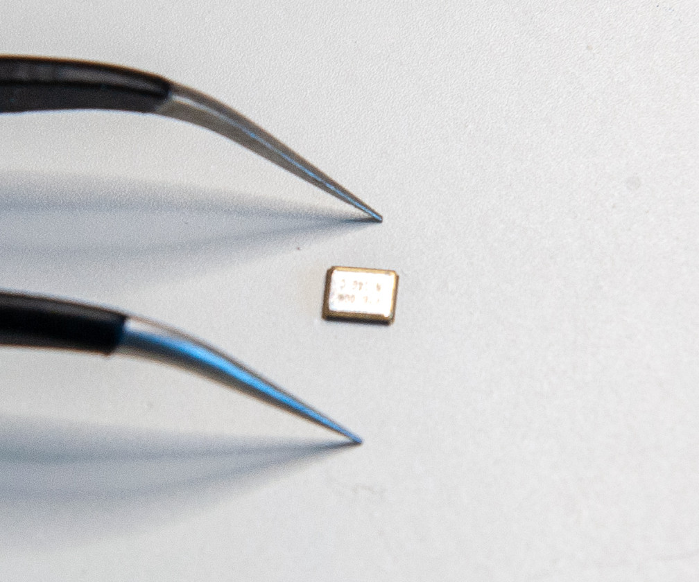
Here’s how a crystal oscillator looks like:

Crystal oscillator

Reference LCSC TME Digikey
16 Mhz Crystal C255909 3225-16m-sr 1923-LFXTAL082071ReelCT-ND

Resistors

To choose resistors, the following characteristics matter:

  • resistance (in Ω)
  • tolerance (in percent)
  • power
  • package size
  • temperature coefficient (short tempco) - or how much the resistance change with temperature. This parameter doesn’t really matter in our use case.

The tolerance is the amount of variation in resistance during manufacturing from one sample to another. The lower the tolerance is, the better the resistor has the indicated value, but the higher the price is.

For most of the applications, a 10% or 5% tolerance doesn’t matter, but for some applications you might want to go down to lower tolerance values like 1% or even 0.1%. I’ve selected 1% tolerance parts, but I believe it is possible to use 5% ones.

The power is the amount of power the resistor is capable to handle without blowing. For this keyboard, 125 mW (or 1/8 W) is more than enough.

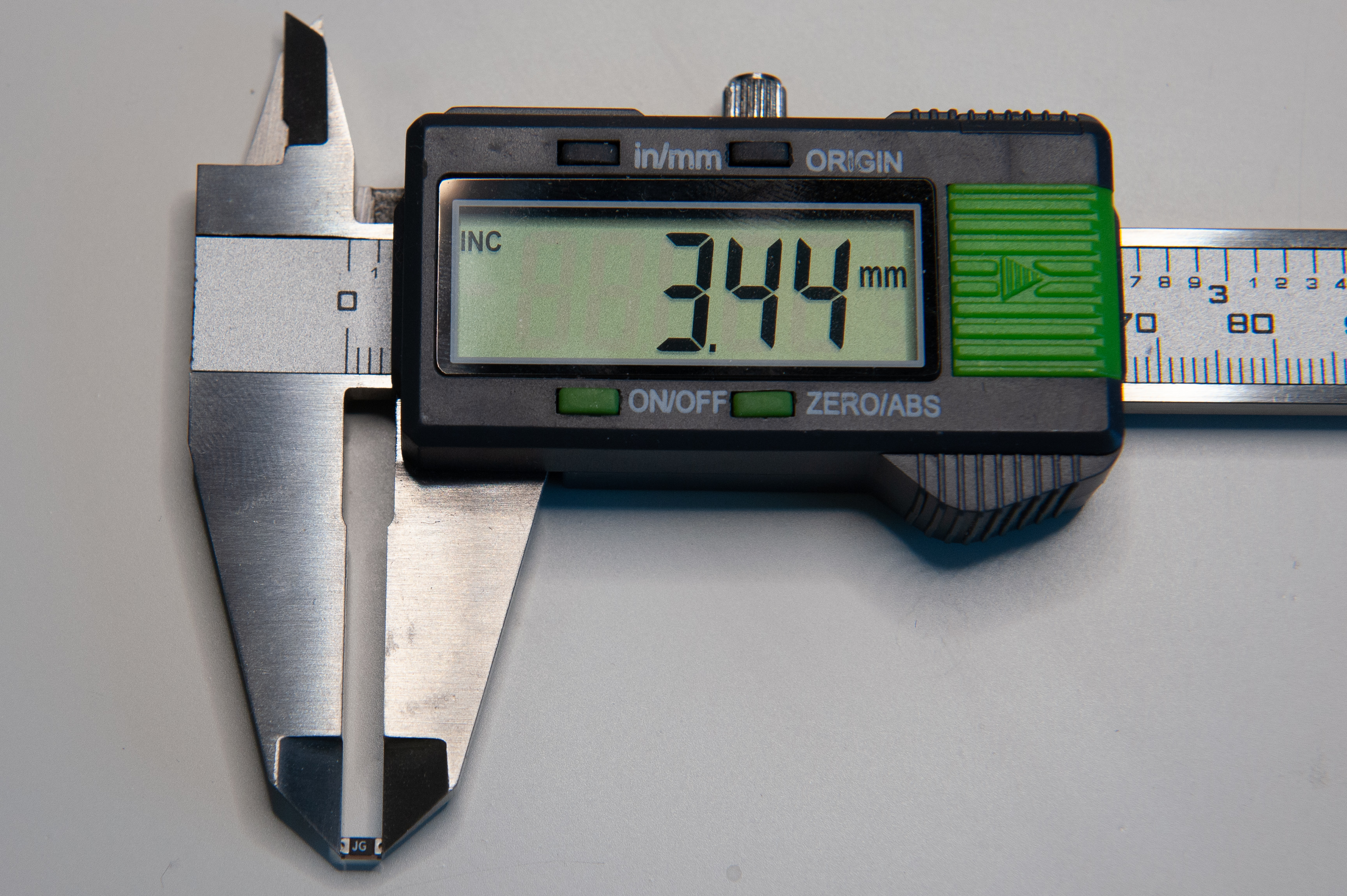
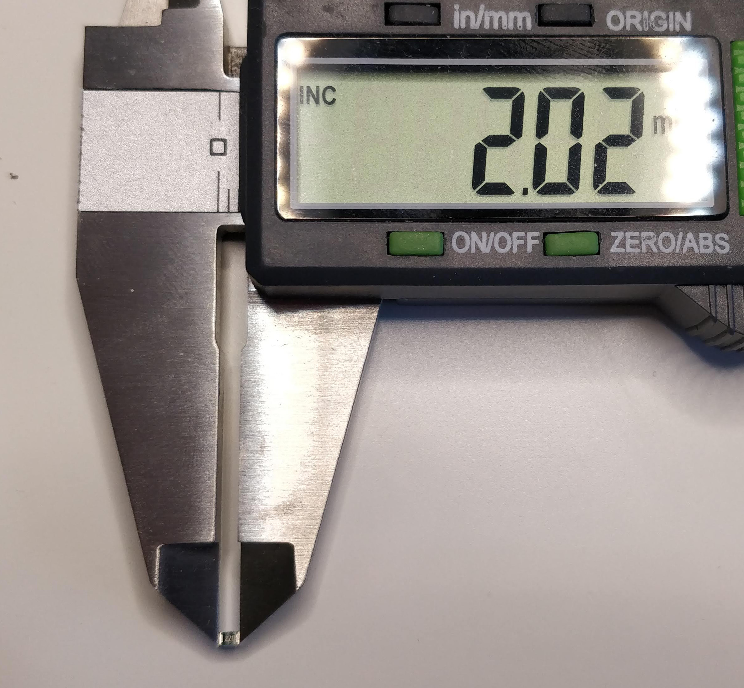
A SMD 0805 resistor (here it’s 22Ω) looks like that (yes that’s the small thing in the caliper):

SND Resistor

Here’s a list of the selected part

Reference resistance LCSC TME Digikey
R1, R2 10kΩ C84376 RC0805FR-0710KL 311-10.0KCRCT-ND
R3, R4 22Ω C150390 CRCW080522R0FKEA 541-22.0CCT-ND
R5, R6 5.1kΩ C84375 RC0805FR-075K1L 311-5.10KCRCT-ND

Note that some of those parts are available only in batch of more than 100 pieces. It is perfectly possible to substitute with parts that are sold in lower quantities as long as the characteristics are somewhat equivalent.

Capacitors

There are many type of capacitors of various conception and technology. For our decoupling/bypass SMD capacitors, MLCC (multi layered ceramic capacitors) are the best.

Here are the characteristics used to describe capacitors:

  • capacitance (in F)
  • tolerance (in percent)
  • max voltage
  • temperature coefficient
  • package size

For decoupling and crystal load capacitors, it is not required to use a very precise capacitance, thus we can use the 10% tolerance. As far as this board is concerned, max voltage can be anywhere above 16V.

The temperature coefficient is (like for resistance) the variation in capacitance when temperature increases or decreases. For capacitors, it is represented as a three character code, like X7R, X5R, where:

  • the first character is the lowest temperature the capacitor will work at (X is -55ºC for instance)
  • the second character is the max temperature (5 is 85ºC, 7 is 127ºC for instance)
  • the last character is the amount of capacitance change over the supported temperature range. R means +/- 15%, but V is about +-85% (ouch).

You might also find C0G (or NP0) capacitors. Those are completely different beasts (in fact it’s a complete different capacitor class), they are not affected by temperature at all.

It’s better to choose R over V variants (ie X7R is better than Y5V for instance). Since our keyboard temperature is not expected to increase considerably, X7R or even X5R can be selected. C0G parts are usually larger and harder to find in package smaller than 1206.

Among manufacturers, you can’t go wrong with AVX, Samsung, Vishay, Murata and a few others. I’ve selected Samsung parts in the table below.

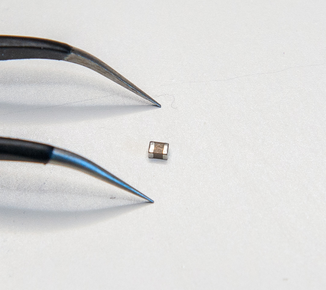
Here’s how a SMD 0805 capacitor looks like:

SMD Capacitor

Reference capacitance LCSC TME Digikey Note
C1-C4 100 nF C62912 CL21B104KBCNNNC 1276-1003-1-ND  
C5 10 uF C95841 CL21A106KOQNNNG 1276-2872-1-ND TME only have the X5R version
C6 1 uF C116352 CL21B105KAFNNNE 1276-1066-1-ND  
C7, C8 22 pF C1804 CL21C220JBANNNC 1276-1047-1-ND lower capacitance are only available in C0G

Ferrite bead

Choosing the right ferrite bead is a bit complex. One has to dig in the various reference datasheets. This PCB needs a ferrite bead that can filter high frequencies on a large spectrum (to prevent noise coupling in GND and ESD pulses). Ferrite beads characteristics are usually given as characteristic impedance at 100 MHz. That doesn’t give any clue about the characteristic impedance at over frequencies. For that, one need to look at the frequency diagrams in the datasheet.

What I know is that, the impedance at 100 MHz should be between 50Ω and 100Ω to be effective to filter out noise and ESD pulses. For the same reason, it also needs to resist to high incoming current.

After looking at hundreds of references, I finally opted for the Murata BLM21PG600SN1D .

Also, since I opted for a 0805 package, its current limit is in the lower part of the scale. I might probably change the PCB in an ucoming revision to use a 1206 sized ferrite bead to have it support higher currents.

Reference LCSC TME Digikey
FB1 C18305 BLM21PG600SN1D 490-1053-1-ND

The remaining parts

Reference LCSC TME Digikey Note
PRTR5V0U2X C12333 PRTR5V0U2X.215 1727-3884-1-ND  
AtMega32U4-AU C44854 AtMega32U4-AU ATMEGA32U4-AU-ND  
HRO-TYPE-C-31-M-12 C165948 not found not found  
Reset Switch C221929 SKQGABE010 CKN10361CT-ND TME doesn’t carry the C&K switch, so substituted by the Alps version

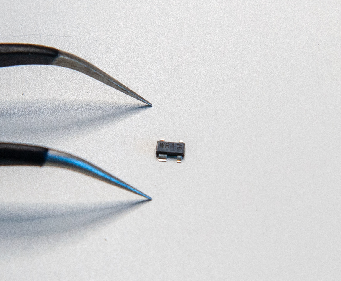
Here’s a picture of the PRTR5V0U2X, notice the GND pin that is larger than the other ones:

PRTR5V0U2X

A bit more information on components

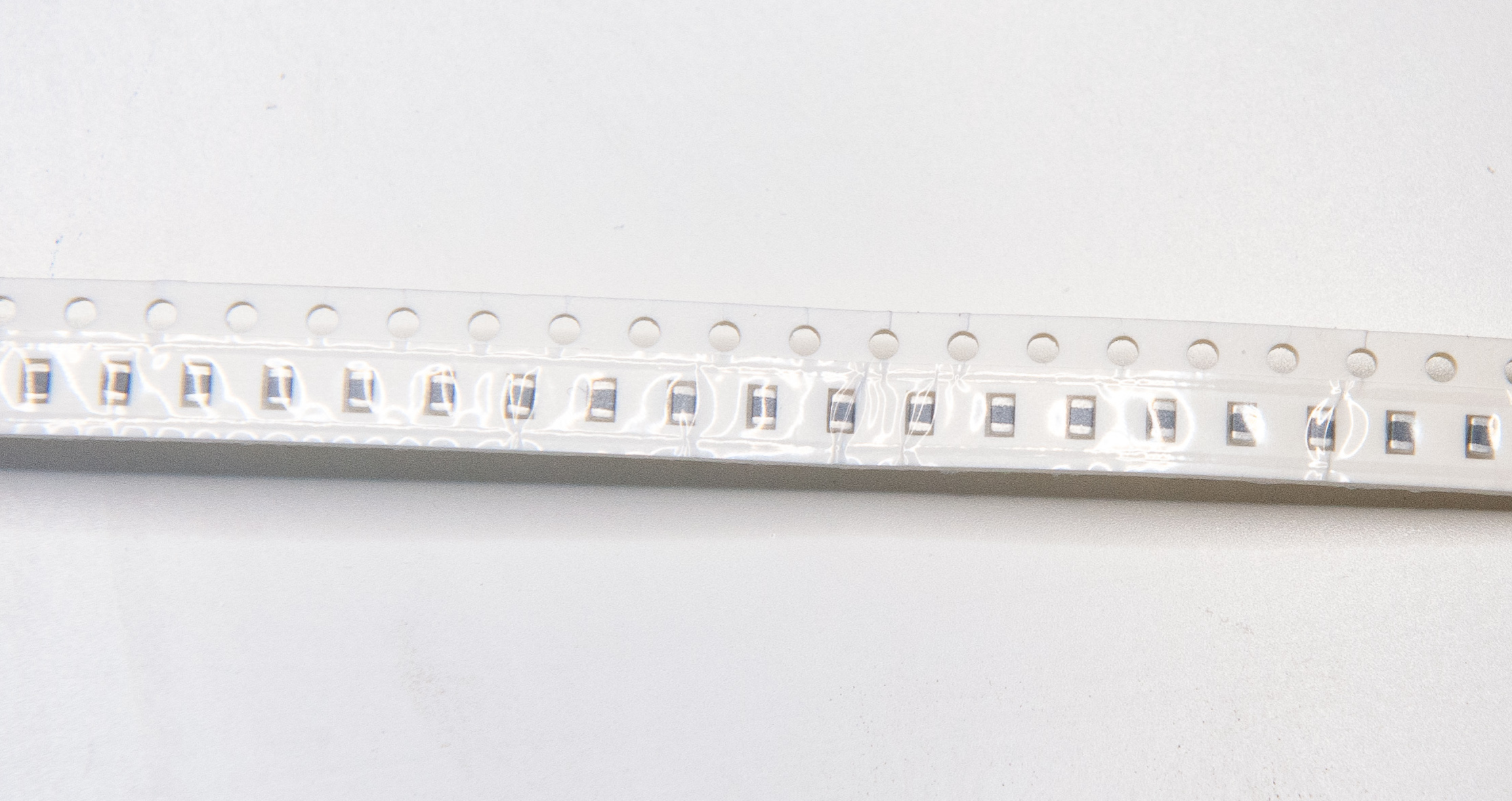
SMD components are packaged in tape reels. If you purchase less than a full reel (4000 to 5000 individual pieces), you’ll get a cut piece of the tape like this one:

Component reel

Those tapes are made of two parts: a small shiny transparent layer on the top (the cover tape) and the bottom the carrier tape. To get access to the component, you just need to peel off the top layer. Since those parts are very small, I recommend to keep them in their tape and peel off only the needed portion of the cover tape.

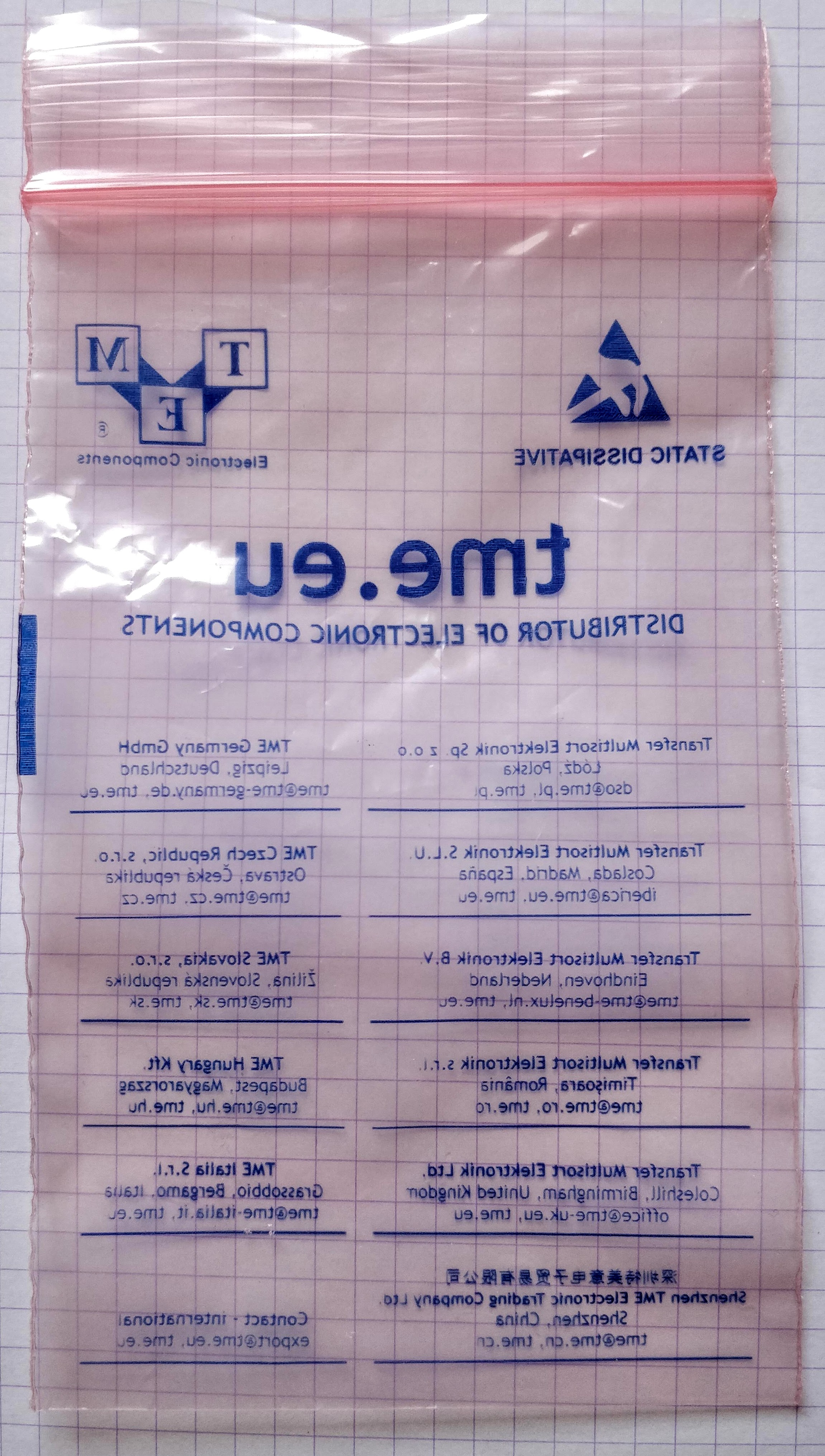
Components are sensible to electrostatic discharge (ESD), that’s why they’re shipped in special anti-static bags. There are two types of anti-static bags. The first kind is dissipative antistatic bags, usually made from polyethylene with a static dissipative coating. They work by dissipating the static charge that could build up on their surface onto other objects (including air) when the bag is touching something else. Those are usually red or pink:

Dissipative bag

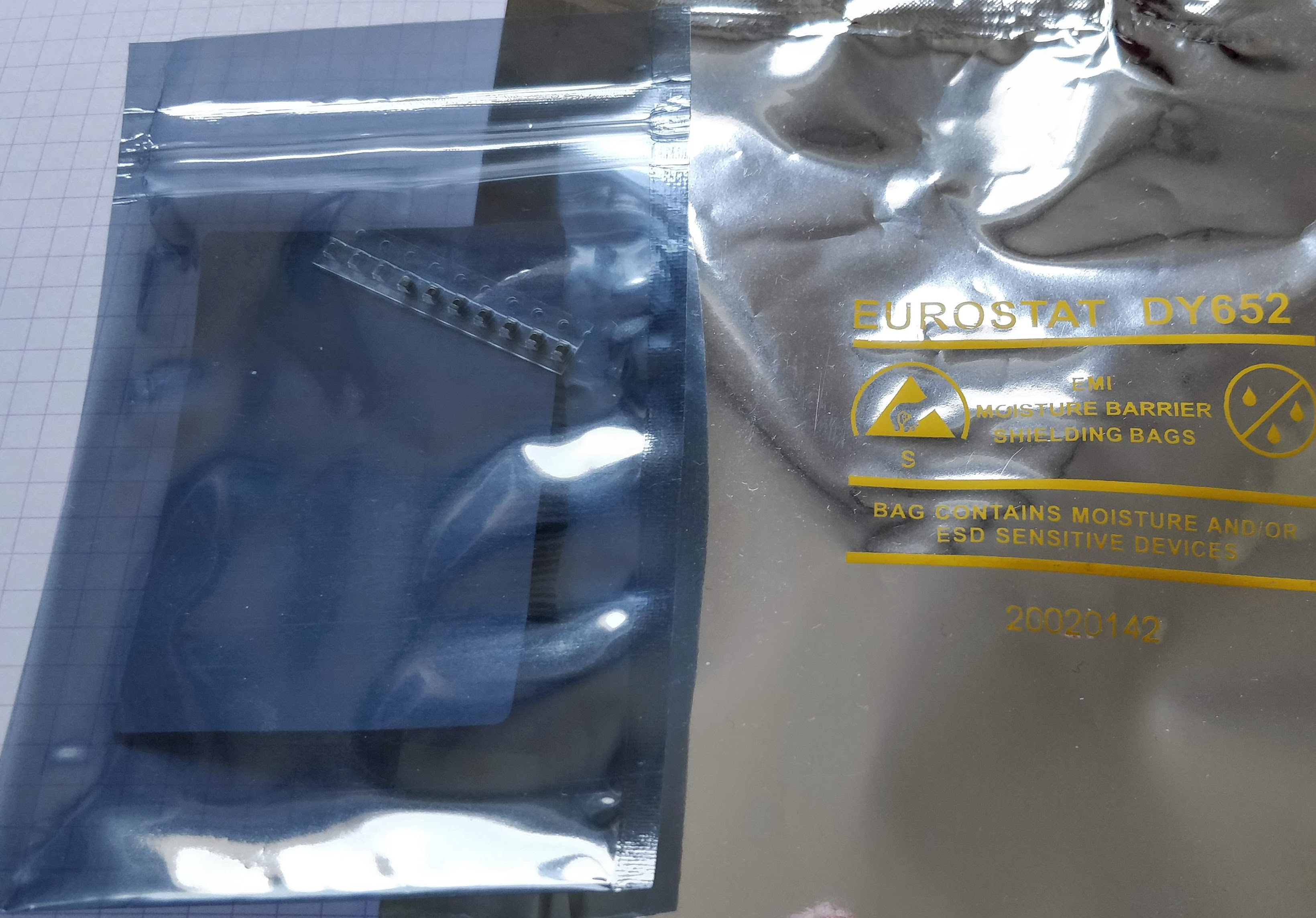
The second kind is conductive antistatic bags, made with a conductive metal layer on top of a dielectric layer. Those bags protect their contents from ESD, because the metal layer forms a Faraday cage. You can recognize those bags because they are shiny and their color is gray or silver:

Conductive bags

Note that those shielded bags are inefficient if the shield is not continuous, so make sure to not use bags with a perforation or puncture.

Components should always be stored in such bags, even for storage. Only remove the components from the bag when you’re ready to solder them on a PCB. And do so if possible in an anti-static environment (ie a specific table or mat is used).

Components should also be stored in a place that is not too humid. Some active components are shipped with desiccant bags inside the ESD protection bag, keep them when storing them as they absorb the excess humidity that could harm the part.

PCB assembly

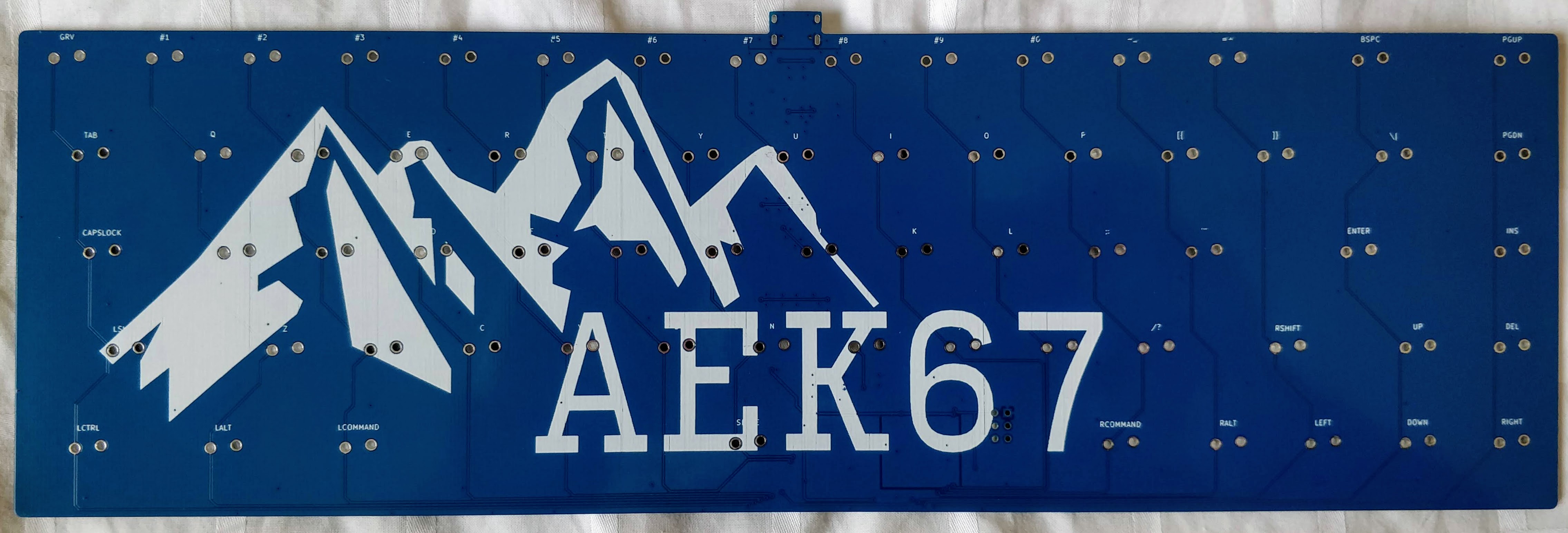
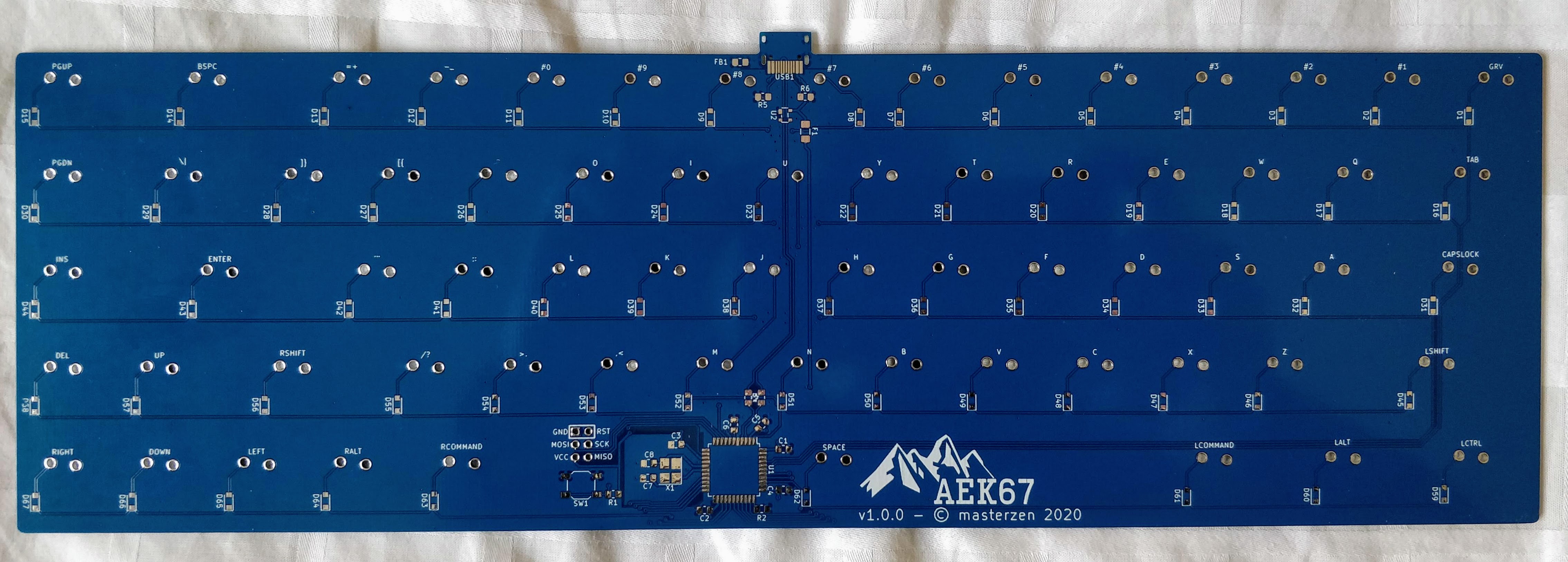
So, it’s mail day: I received the PCB:

AEK67 front PCB

AEK67 back PCB

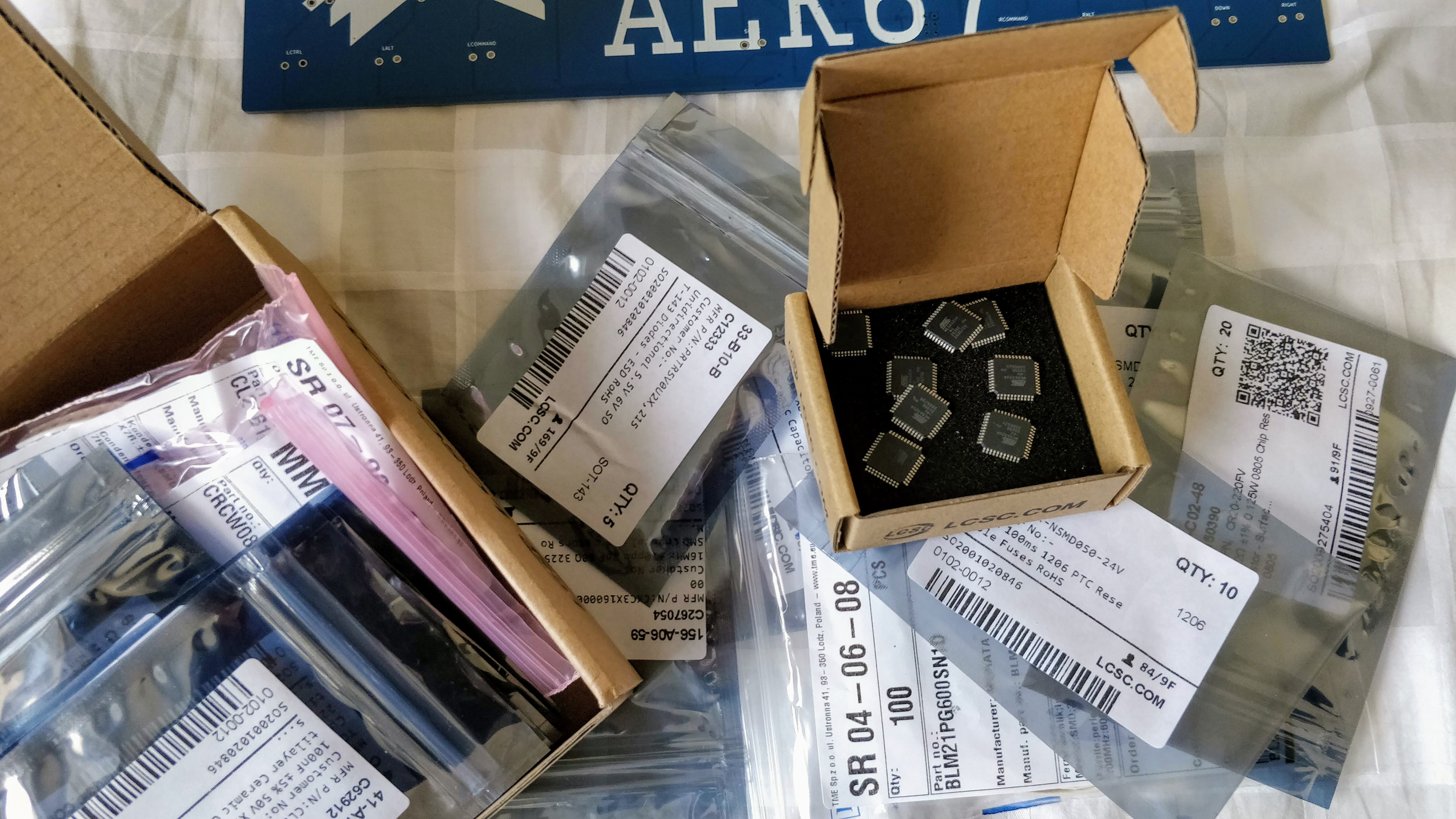
and the components (see the AtMega32U4 in the cardboard box in the center):

SMD components

I’m now ready to assemble the PCB, that is solder all the components.

The tools

To do that the following tools are needed:

  • ESD safe tweezers
  • a soldering iron & tip
  • tools to clean the iron
  • solder
  • extra flux
  • desoldering tools
  • magnifying tools

That’s the minimum required. Of course if you can afford a microscope or a binocular that would be awesome (I don’t have one, so that’s not strictly needed)

ESD tweezers

As I’ve explained earlier, electronic components can be destroyed by electro-static discharges. The human body is able to accumulate charges (for instance on walking on a carpet) and when touching another object discharge into it. Thus it’s important to prevent ESD when manipulating components.

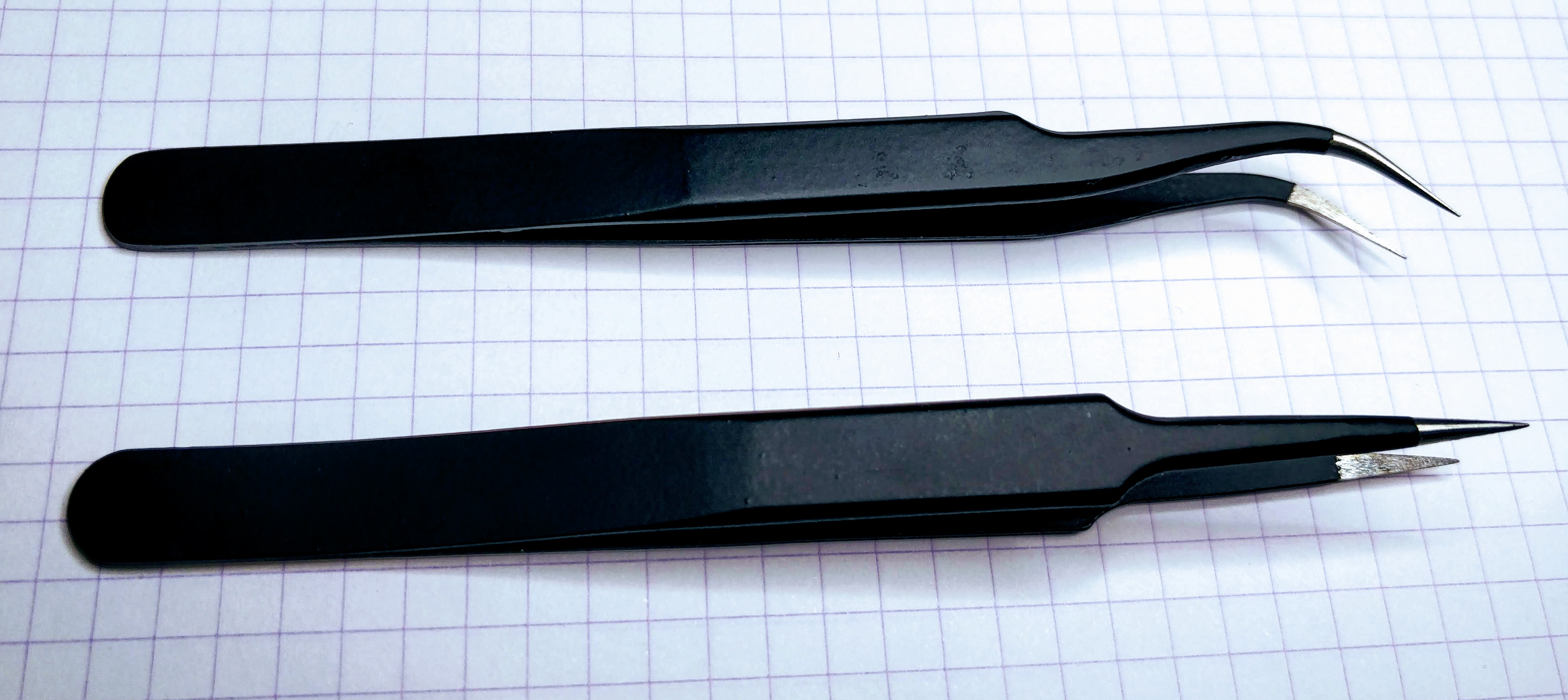
To be able to place precisely the component on the PCB while soldering it, and also hold it while the solder solidifies, we need a pair of electronic tweezers. Since usually tweezers are made of metal, they would conduct the static charge to the component or the board. ESD tweezers are metallic tweezers that are coated with an non-conductive anti-static material, preventing the charges to be transferred from the body to the component.

You can find cheap tweezer sets at Amazon or more expensive ones at the previous vendors I cited for sourcing components.

Here are mine:

ESD Tweezers

Soldering iron

I’ll recommend using a temperature controlled soldering iron, especially for soldering very small parts. One good choice would be either the Hakko FX888D, the FX951 or any other serious temperature controlled stations (among those made by Weller or Metcalf for instance). Hakko stations can be purchased in EU from batterfly.

You’ll also find Hakko T12 compatible stations on Aliexpress (like the KSGER T12), those are nice and inexpensive, unfortunately their PSU is rigged with defective designs that make them not as secure as they should (they probably wouldn’t pass CE conformity as is). I thus won’t recommend them (see this video for more information).

Then finally you can find standalone USB powered soldering irons like the TS80P or TS100. Those are very lightweight and have a custom opensource firmware superior to the original. They have a drawback: they’re not earthed by default and thus not completely ESD safe. The risk is a potential ESD destroying the SMD components that are being soldered. Regular wall-in soldering irons have the heating tip earthed and thus can’t build up an electrostatic charge. Moreover, those USB soldering iron are known to leak current when used. This can be fixed by adding an earth connection from the iron to common earth which requires a specific cable from the iron to an earth point (or at least a common potential point between you, the iron and the PCB, which can be done with specific anti-static workbench or mats). Some TS80P kits contain such earth grounding cables, some other not. I’m reluctant to recommand those for these reasons.

I myself have an inexpensive Velleman station (made in China). It’s certainly not the best, but it does its job reasonably well and is CE certified.

Rergarding soldering iron tips, you can find many different ones and it will depend on the soldering iron you’ve got. There are tons of different Hakko tips (here for the T12 tips). In this brand, the recommended ones for SMD parts are shapes D, BC/C and B. Regarding tip size, you can’t go wrong with D12 (or D16), B2 and BC2.

Iron tip cleaning

The soldering iron tip is critical for the tool performance. If it can’t perform its function of transferring heat to the solder joint, the soldering iron will not be efficient. Thus it is important to take care of the tip to prevent any soldering issues.

Soldering tips will wear throughout the time of use and will probably have to be replaced at some point. Careful tip hygiene will extend its life.

A particularly recommended tool is a metallic wool, like the Hakko 599b or a cheap clone:
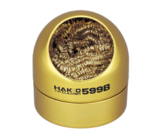
Hakko 599b

Those cleaners are preferred other wet sponges, because the sponges will reduce the temperature of the iron tip when used, which means the tip will contract and expand quickly during cleaning. Frequent use of the sponge will cause metal fatigue and ultimately tip failure. Metallic wool cleaners are very effective at removing the dirt, contaminants, and flux or solder residues.

The idea is to prevent oxidation, for this, clean the tip before using the soldering iron on a new component, not after. While the tip is not used between two components, the flux and solder will protect the tip from oxidation.

When you’ve finished your soldering job, clean the tip with the metallic wool and tin the tip. It is possible to buy a tip tinning box. Most large solder manufacturer produce this kind of product, mine is this reference:

MgChemicals tip tinning

You might see recommandation of applying solder on the iron tip after use. This works fine if the solder contains a rosin activated flux (see below). But for no-clean solder (the majority of solder nowadays), the flux is not aggressive enough to remove or prevent tip oxidation. I recommend using a special tip tinner as the one above.

Solder

The solder is an alloy that melts from the heat of the iron to form the joint between the PCB pad and the component. It is important to purchase a good quality solder (especially if you have to perform some rework). There are two types of solder, those that contains lead and the lead-free variant. The latter is better for health and environment, but might be harder to use because it requires a higher soldering temperature. The former is easier to deal with, but is forbidden in EU because of RoHS compliance (it’s still possible to purchase leaded solder though).

Solder should also contain flux (even though as you’ll see later, adding flux is necessary to properly solder SMD components). The flux purpose is to clean the surfaces so that the solder wet correctly and adheres to the pad and components.

Solders are described by their content, like for instance Sn60Pb40, Sn63Pb37 or Sn96.5Ag3Cu0.5. It’s simply the percentage of their constituents. For instance Sn63Pb37 is an alloy made of 63% of tin and 37% of lead. Unleaded solder is mostly made of tin and silver, and sometimes a low level of copper.

For beginners, Sn63Pb37 would be the simplest solder to use. It is an eutectic alloy. This means that the alloy has a melting point lower than the melting point of any of its constituents (or any other variation mix of tin and lead), and that it has a very short solidifying phase. This makes this kind of solder easy to work with.

Unleaded solder have a higher melting point (around 220ºC) that might take time to be accustomed to.

Well, that doesn’t give you the temperature at which you’ll have to solder the components. For SMD parts, with leaded solder, I usually set my iron between 310ºC and 320ºC. This is high enough to quickly heat the pads. Lower temperature would mean to keep the iron tip longer on the pad and component with the risk of heating too much the component. Unlike common thought, the heat conductivity of metal decreases with temperature, which means that using a lower temperature would mean more heat accumulating in the component (because of the iron tip staying longer on the pad and component), and an increased risk of destroying it.

For unleaded solder, the recommended iron temperature is around 350ºC. But it also depends on the iron tip used. Smaller iron tips have a lower heat transfer surface and thus, you will need to use a larger temperature and longer soldering to achieve the same effect as with a larger tip.

Using a solder containing rosin flux is also recommended. The metallic surfaces in contact with air will oxidize, preventing the chemical reaction that will bond them to the solder during the soldering. Oxidization happens all of the time. However, it happens faster at higher temperatures (as when soldering). The flux cleans the metal surfaces and reacts with the oxide layer, leaving a surface primed for a good solder joint. The flux remains on the surface of the metal while you’re soldering, which prevents additional oxides from forming due to the high heat of the soldering process.

As with solder, there are several types of flux, each with their own key uses and limitations:

  • Rosin (R): This is the most known one. It is a compound which was made originally from pine trees, but is now synthetic. Its liquefaction temperature is lower than the solder one, so it flows first. It becomes acid when liquified which allows its cleaning action before the solder melts to form the joint. The PCB needs to be cleaned after use with isopropyl alcohol (IPA) to remove residues.
  • No Clean Flux (NC): It’s another big category. No-clean flux residue don’t need to be removed from the PCB. This flux should even be called “can’t clean” instead of no-clean, because if you want to remove residues, it’s very hard to do so and requires the proper solvent. The flux residues are usually transparent and non-conductive, so it’s fine to leave those on the board. Most solder nowadays contain NC flux.
  • Rosin Mildly Activated flux (RMA): RMA is a compound made of rosin, solvents and a small amount of activator. RMA flux is not very aggressive and should be used with easily solderable surfaces (so it works well for SMD). The clear residue is normally non-corrosive and nonconductive. It might not be necessary to clean it after work.
  • Rosin Activated flux (RA): Activity is higher than RMA, and should be used on oxidized surfaces. It is corrosive so it should be cleaned as soon as possible after work (with the appropriate solvent). The RA category also contains water soluble versions that also are highly corrosive, but can be cleaned with water (also because it’s conductive). Those are used to solder on difficult surfaces like stainless steel.

It’s still not finished about solder. How to choose the appropriate solder diameter? A good compromise for soldering a combination of SMD parts and through-hole components is 0.7 or 0.8mm.

Finally, soldering is a health hazard, so make sure to read the following important warnings:

  • Make sure to wash your hands thoroughly after soldering.
  • Solder in a ventilated room, do not inhale soldering smoke, purchase a fume absorber
  • avoid eating, drinking, smoking in solder areas to prevent solder particulates to enter your body

Among the various brands of solder, those are known to produce good solder: MgChemicals, Kester, Weller, Stannol, Multicore, Felder, MBO etc. For a thorough comparison of several brands and models, you can watch SDG video: What’s the best solder for electronics

If you solder more than occasionally it might be worth investing in a small fume extractor like this Weller WSA350 or the Hakko FA-400.

Flux

The flux contained in the solder will not be enough to solder SMD parts. It is recommended to add extra flux before soldering the components, especially for ICs or fine pitch components (see below for the different techniques).

Flux exists in several forms:

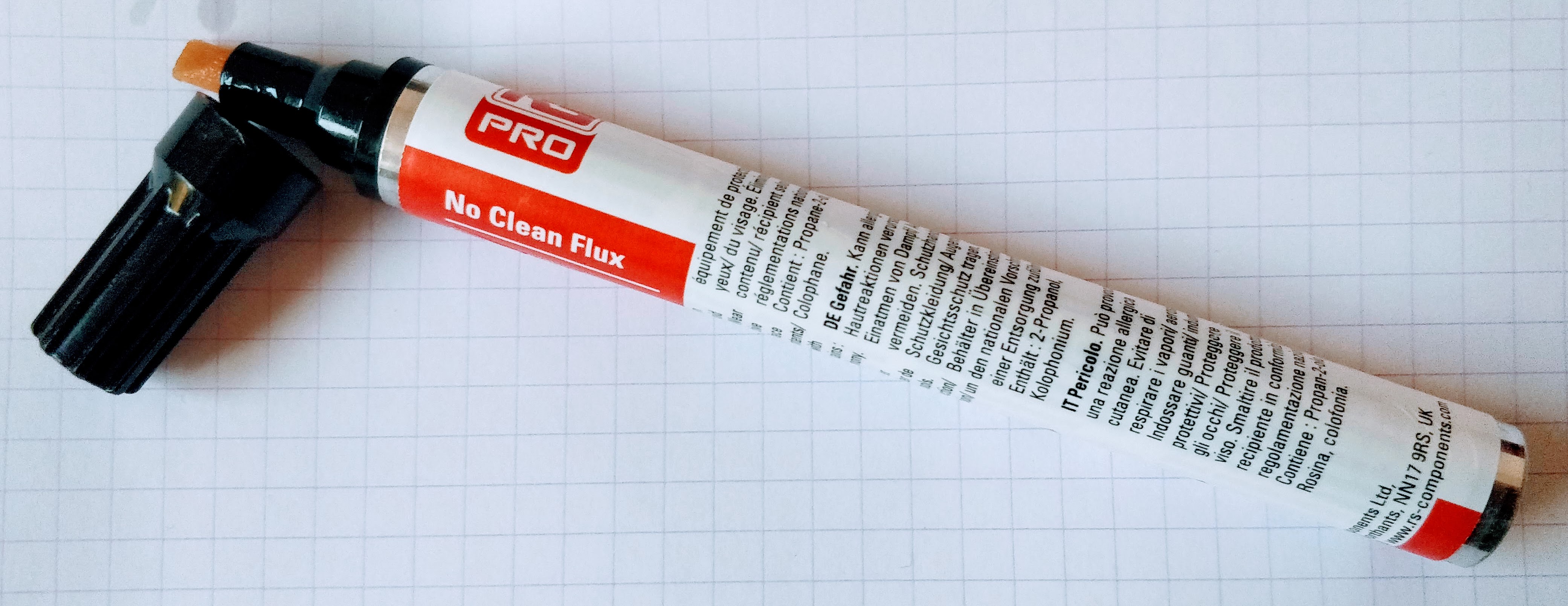
Here’s a flux pen: Flux pen

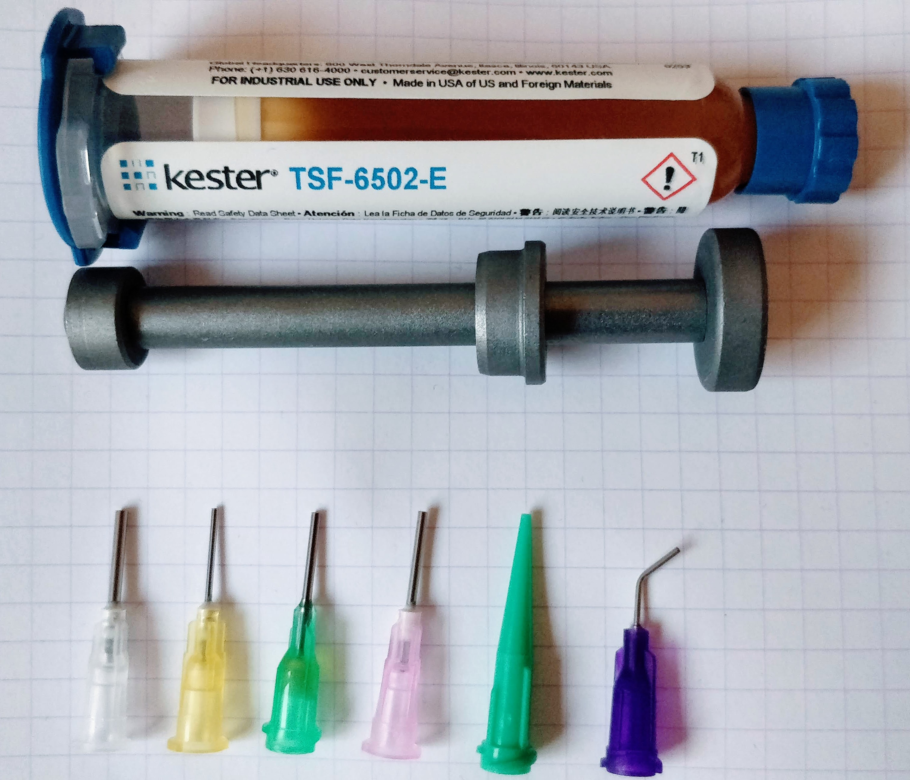
And a flux serynge (ready to be used): Flux serynge

A note on flux serynge: most of them are sold without an applying nozzle and a plunger. That’s because professionals are using special dispensers. So do not forget to also purchase a plunger (they are dependent on the serynge volume) and nozzles. The nozzles are secured to the serynge by what is called a luer lock, which is a kind of threading inside the serynge.

Serynge, plunger and nozzles

I recommend getting a flux paste serynge, as the flux from the pen is more liquid and tends to dry more quickly than the paste.

For a comparison of fluxes, you can watch the SDG video: what’s the best flux for soldering

Desoldering tools

Mistakes happens :) so better be ready to deal with them. It might be necessary to remove extra solder or remove a component misplaced by mistake. Without investing a lot of money in a desoldering iron or station, it is possible to get inexpensive tools that will help.

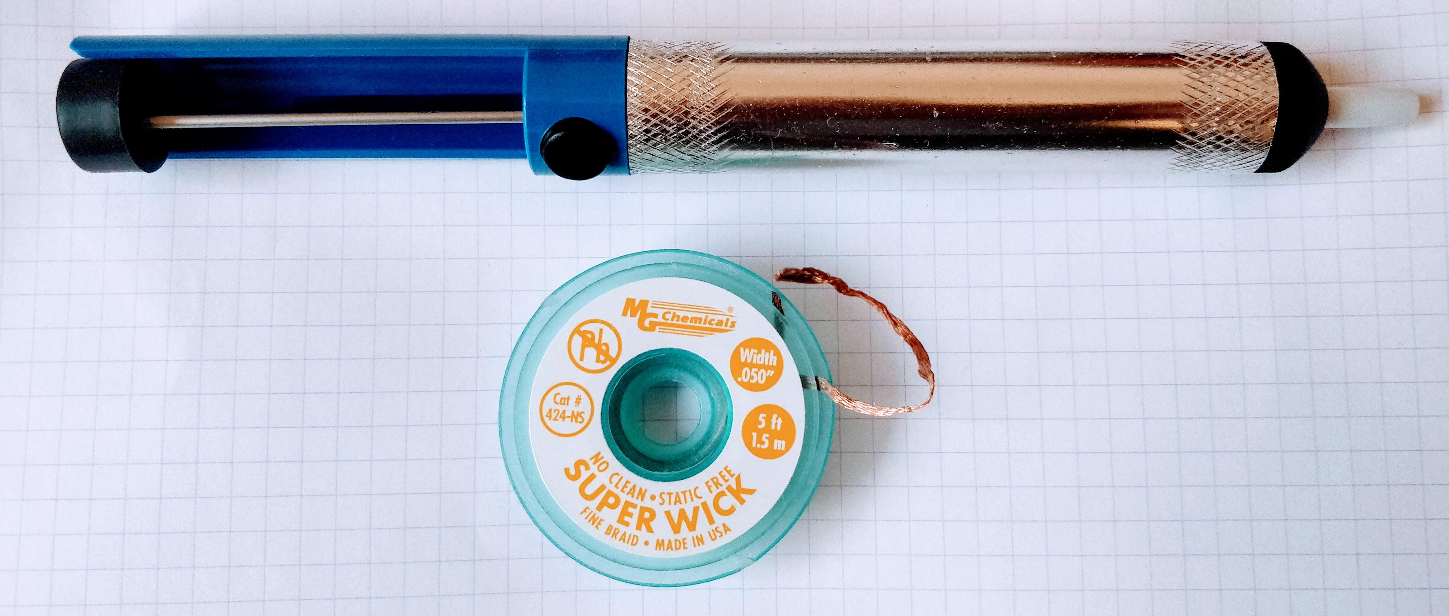
Let me introduce you to the desoldering pump and its friend the solder wick:

Desoldering tools

The top object in the picture is a desoldering pump. You arm it by pressing down the plunger. When released with the button, it will suck up the melted solder. It is to be used with the soldering iron heating the excess solder, then quickly apply the pump.

The solder wick is to be placed on the excess solder, then put the iron tip on top of it, the solder will melt and the wick will also suck it. It might be necessary to add a bit of flux before.

Magnifying tools

Finally the last tool needed when soldering small SMD parts is a good lamp with an integrated magnifier glass. As seen earlier, most of the component are less than 3 or 2 mm long, so it is hard to properly see them when soldering (unless you have very good eyes, which is not my case).

Of course getting a binocular or a microscope would be awesomely useful, but those are quite expensive (especially if you want quality). Instead I think a good magnifying glass lamp can do the job quite efficiently. The best ones are the Waldman Tevisio, unfortunately they are very expensive. It is possible to find cheaper alternatives on Amazon or one of the parts vendors I previously cited (I got myself this RS Online model).

The magnifying lens of such lamp is expressed in diopters. You can compute the magnifying ratio with the D/4+1 formula. A 5d lens will provide a 2.25x magnification. This is enough to solder small parts, but my experience (and bad eyes) show that when there’s a small defect its quite hard to have a good view of it (like when there’s a small bridge on two close pins on high-pitched ICs).

That’s why I also recommend getting a standalone small jewelry 10x magnifying glass. The Japanese Engineer SL-56 does an excellent work.

Assembling the PCB

Enough about the tools, let’s see how to assemble the components on the PCB. First let me explain how to solder SMD parts. The technique is the same for 2 pads or multiple pads, except for fine pitch ICs which will be covered afterwards.

I’m very sorry for the bad pictures and schemas that appears in the two next sections. I unfortunately don’t have a macro lens for my camera, and my drawing skills are, well, very low :)

Soldering techniques

2 pads component soldering technique

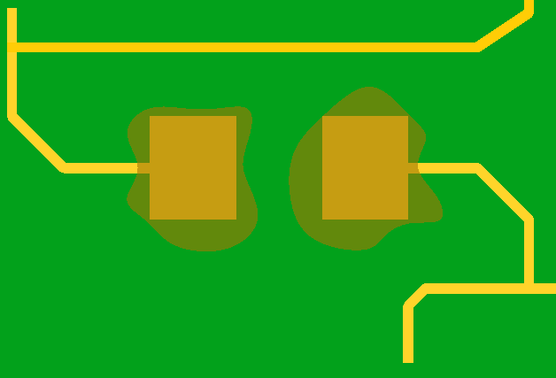
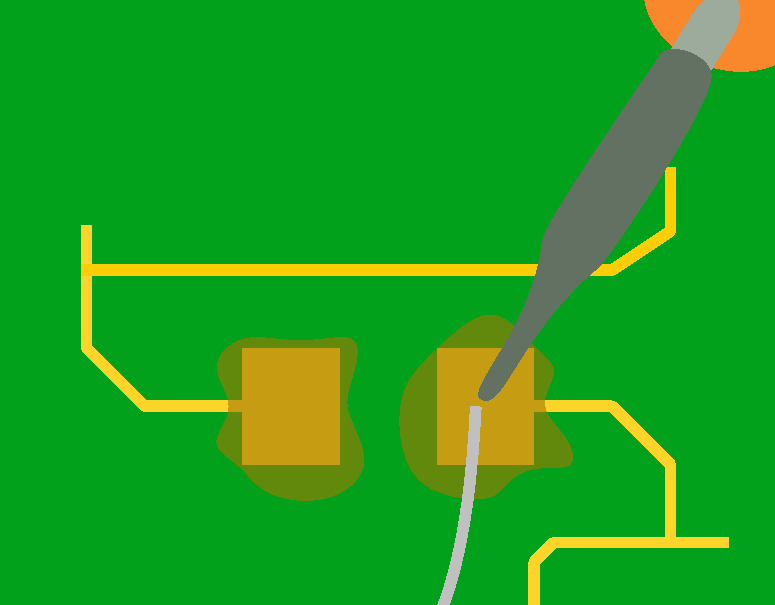
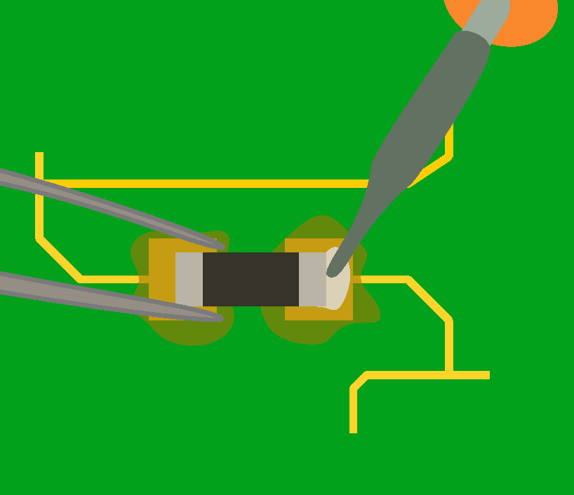
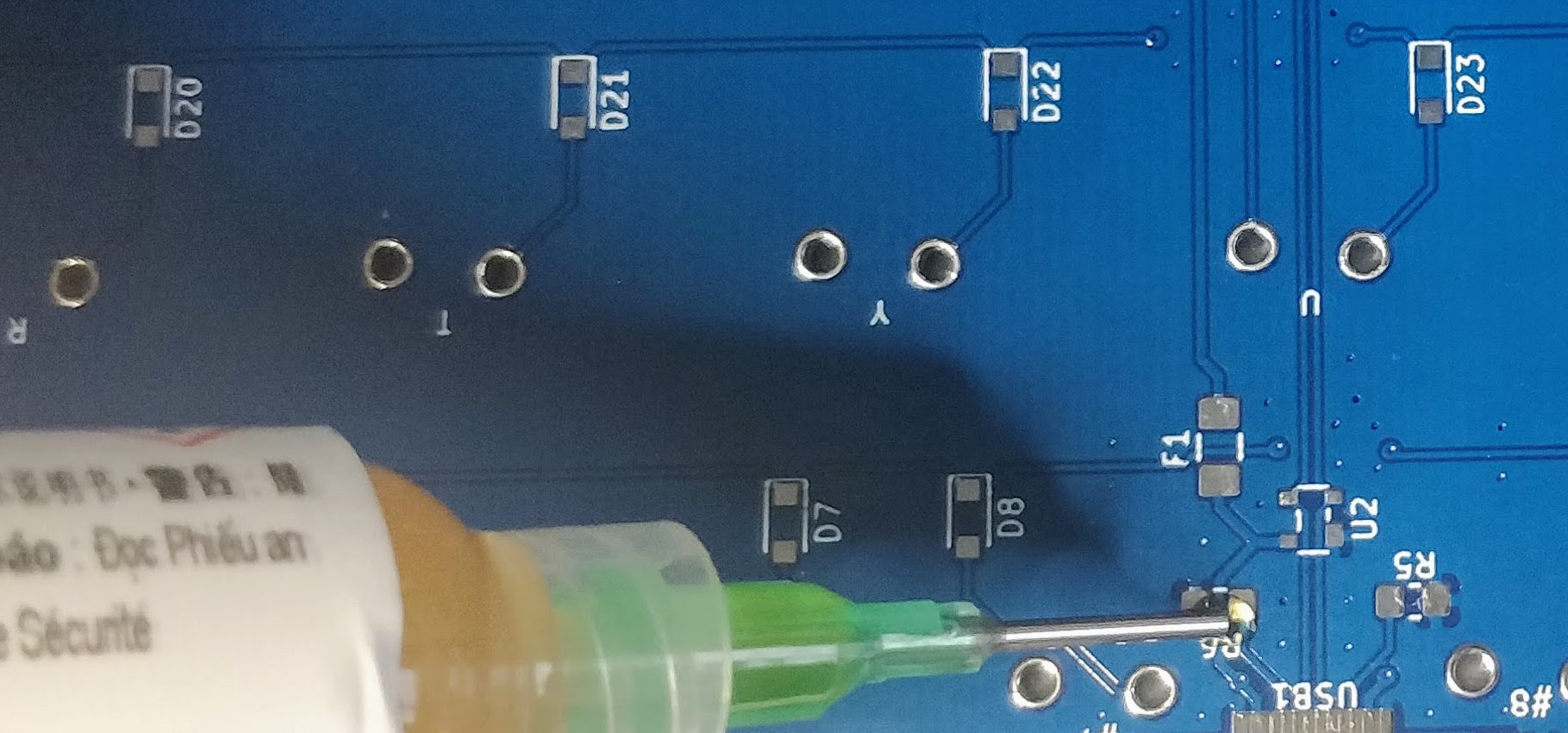
First apply a small amount of flux paste on both pads:

Adding flux on pads

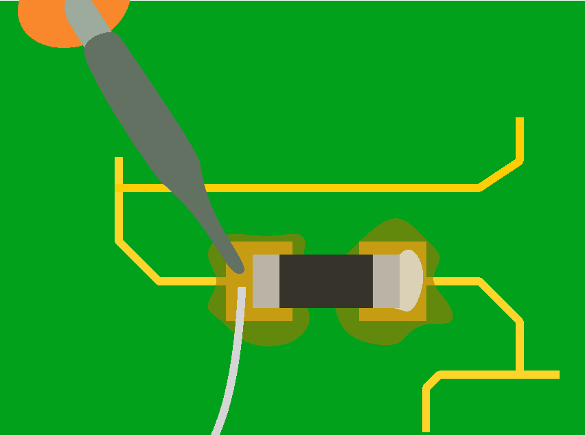
Next, wet a small amount of solder on one of the pad with the soldering iron:

Adding a small amount of solder on pad

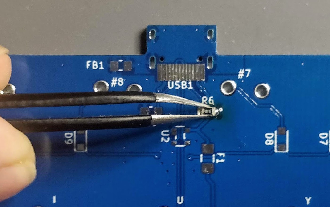
Then place the component with the tweezers, hold it firmly in place and reflow the solder on the pad until the joint is formed:

Soldering first pad

Once the solder has solidified, solder the other pad normally:

Soldering second pad

On a real component (here a 5.1k resistor near the USB receptacle), this give these steps:

Adding flux: Adding flux on pads

Apply some solder on one of the pad: Adding a small amount of solder on pad

Place the component: Soldering first pad

And since I don’t have three hands (and need one to take the picture), I soldered the first pad without holding the component (most of the time, when there’s enough flux the component will place itself correctly): Soldering first pad, next
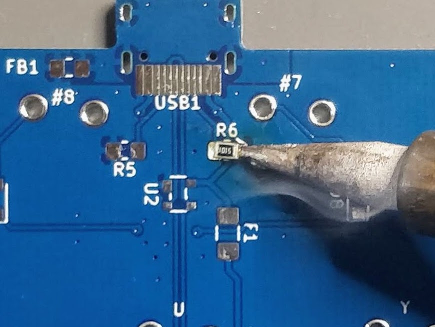
And the result (granted the component could be better aligned, the picture has been taken through the SL-56 magnifying glass): The result
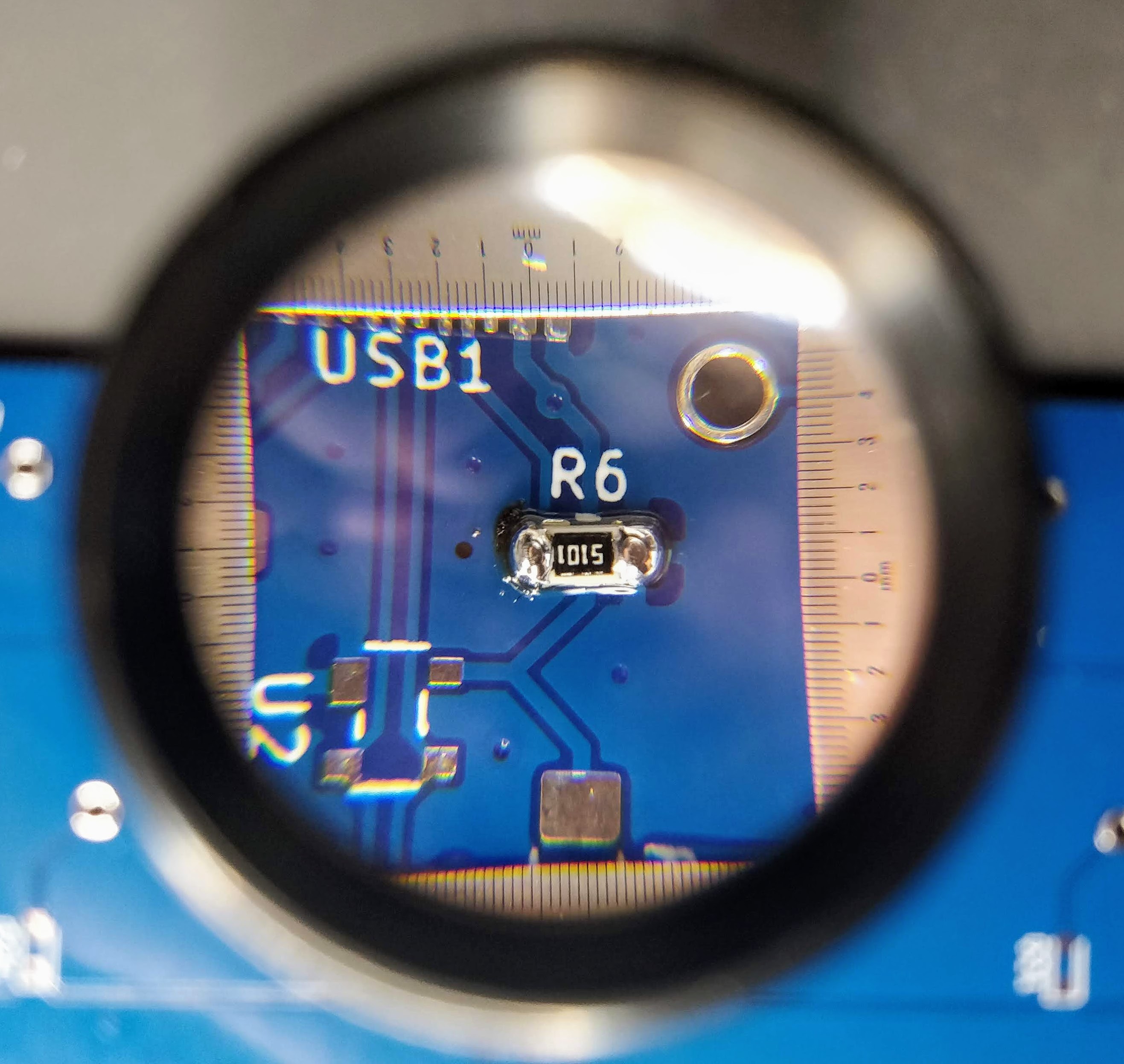
This very same technique can also be applied to 3 or 4 legged components. Start by soldering one pin, making sure the component is correctly placed, then add solder on the other pins.

Drag soldering

The previous soldering technique doesn’t work for fine pitch components like ICs or the USB receptacle on this PCB. For this we need a different technique: drag soldering.

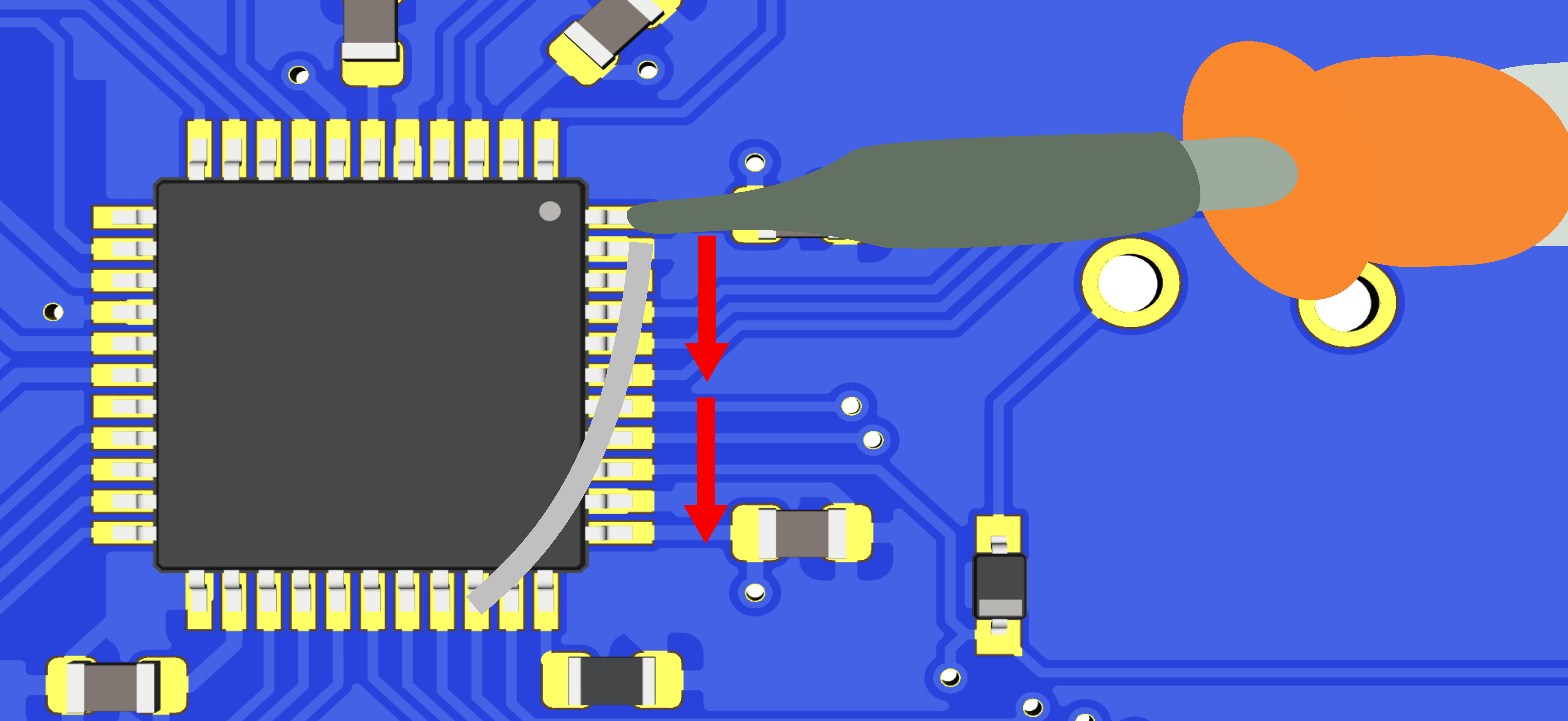
The drag soldering technique consists in first soldering 2 opposite pads of an IC, then to drag the soldering iron tip and solder along the pins relatively quickly. The flux and soldermask will do their job and solder will flow only on the metal parts. Bridges can happen if there’s too much solder or the iron tip is not moved quickly enough. That’s where the solder wick is useful to remove the excess solder.

To properly drag solder, first add solder on two opposite pads of the IC. Then carefully place the IC with the tweezers, hold it firmly and reflow those two pads (this is the same technique as for 2 pins components). When the solder solidifies and form a joint, the IC is secured at the right place, and we can start drag soldering.

Here’s a small schema illustrating the technique:

Drag soldering illustrated

You’ll find the technique shown in this drag soldering video. Notice the tip shape used in the video (equivalent to a T12 BC), and how the solder is put under the tip. If you don’t use a slanted tip, you can still put some solder on the iron, or use what I described above, moving the solder at the same time as the iron tip.

Soldering the PCB

So I’m ready to solder the PCB with the aforementioned techniques. Since it’s harder to solder fine pitch components, it’s better to start with them. There’s nothing worst than soldering all 2-pads components, then failing soldering the most complex one and having to thrash the board.

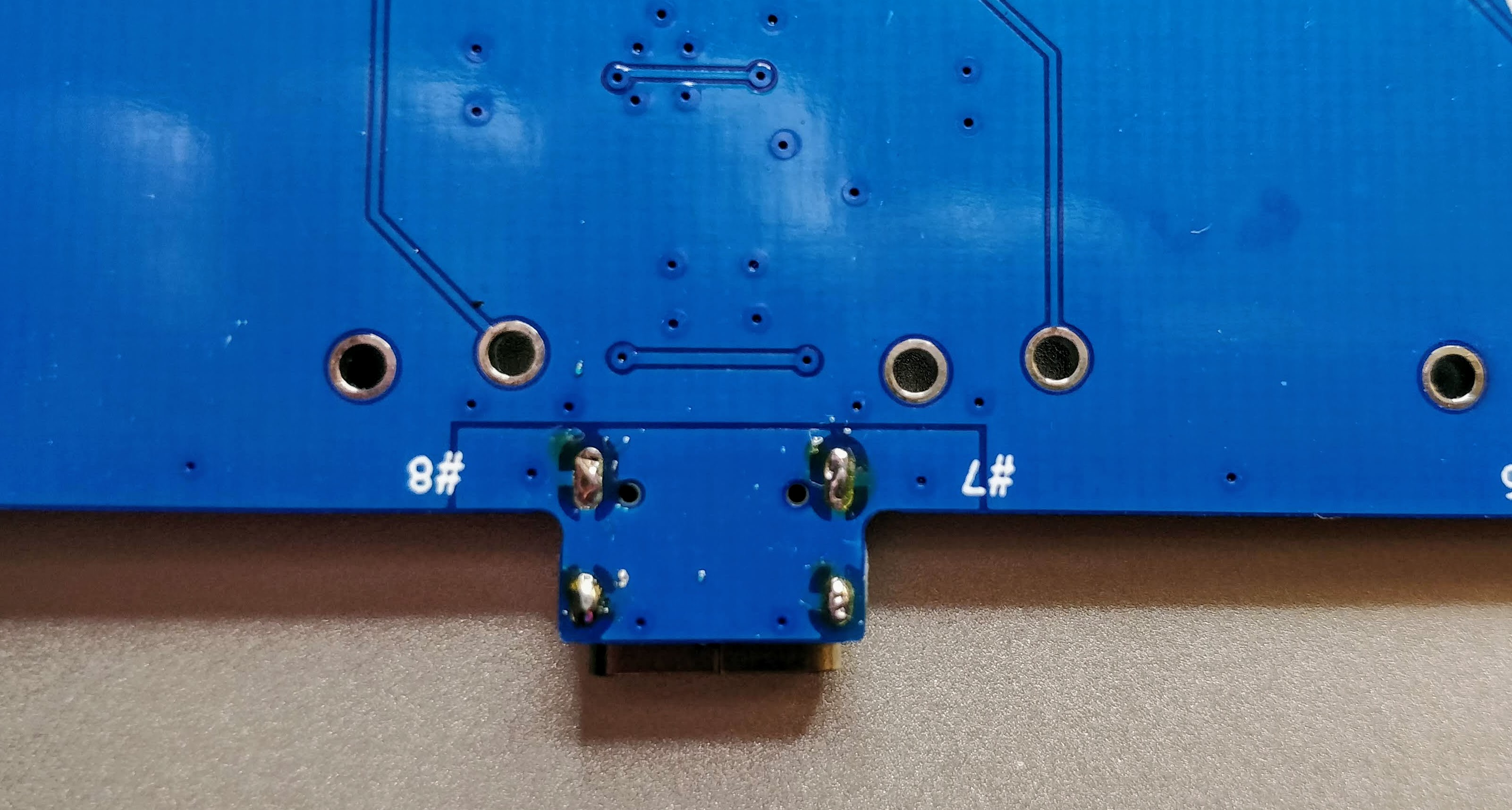
My advice is to start by soldering the USB connector first. Place it so that the small pins enter the board and solder on the front side. The USB connector is then now in place and the small pins are exactly placed on top of the pads on the back side of the PCB:

Soldering USB connector

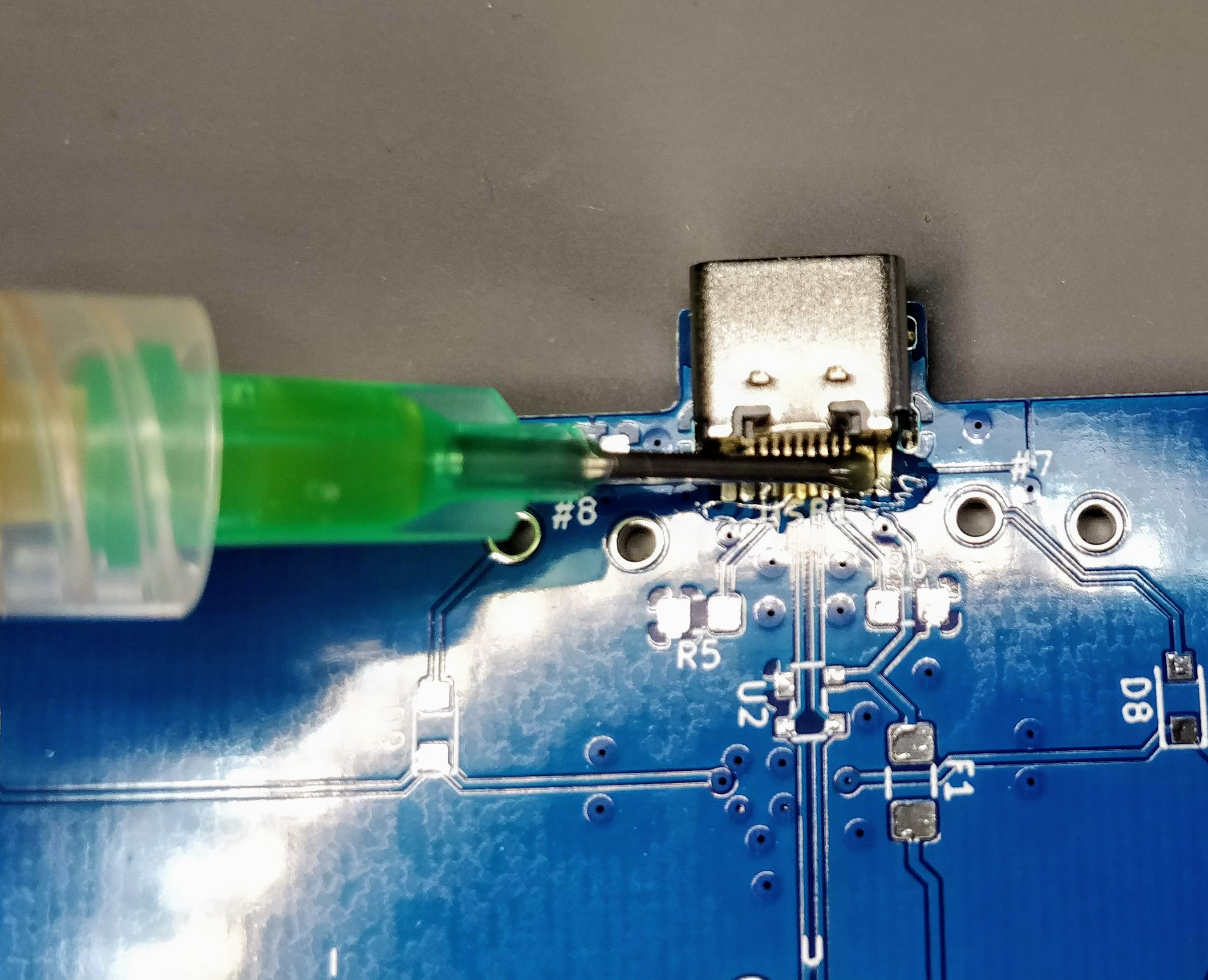
Then apply some flux paste on the other side accross the pins:

Adding flux on the connector

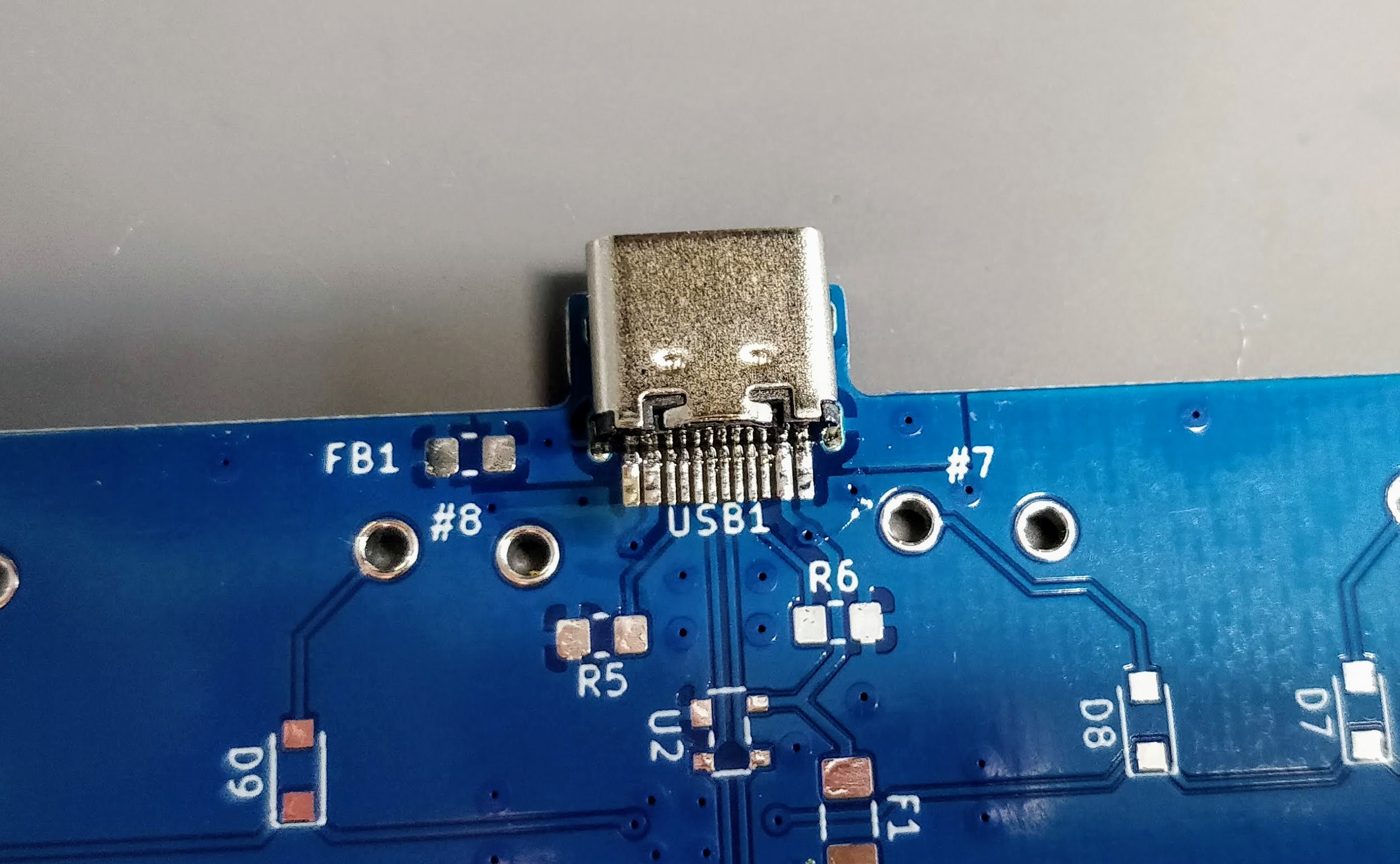
And drag solder the connector. This will give this (flux have been removed in the following picture):

Drag soldered connector

Now is a good time to visually inspect there’s no bridge. Then it might also be a good idea to test that there’s no Vcc and GND short with a multimeter. Most multimeter (even the cheapest ones) have a “diode test” or continuity mode. In this mode the multimeter sends a very small current across the probes and measures the voltage. When the resistance is very small (if there’s electrical continuity between them) the multimeter will produce a beep. If there’s no continuity there won’t be any beep and the screen will show something specific (on mine it displays 1 which is very misleading).

With the multimeter in continuity testing mode, put the black probe on one of the GND pin and the other on one of the Vcc pin (or reverse, it doesn’t matter). There shouldn’t be any continuity (or beep). If there’s continuity, it means there’s a bridge that needs to be found and repaired by adding flux and using the iron tip or with the help of solder wick. You can test the other pins, there shouldn’t be any continuity except for pins that are doubled (D+/D-, GND, Vcc).

If everything is OK, the next step is to solder the AtMega32U4 MCU. First make sure to check how it should be placed. The silkscreen printed at the back of the board contains a small artifact indicating where pin 1 is. On the chip, the pin 1 is the pin close to the small point.

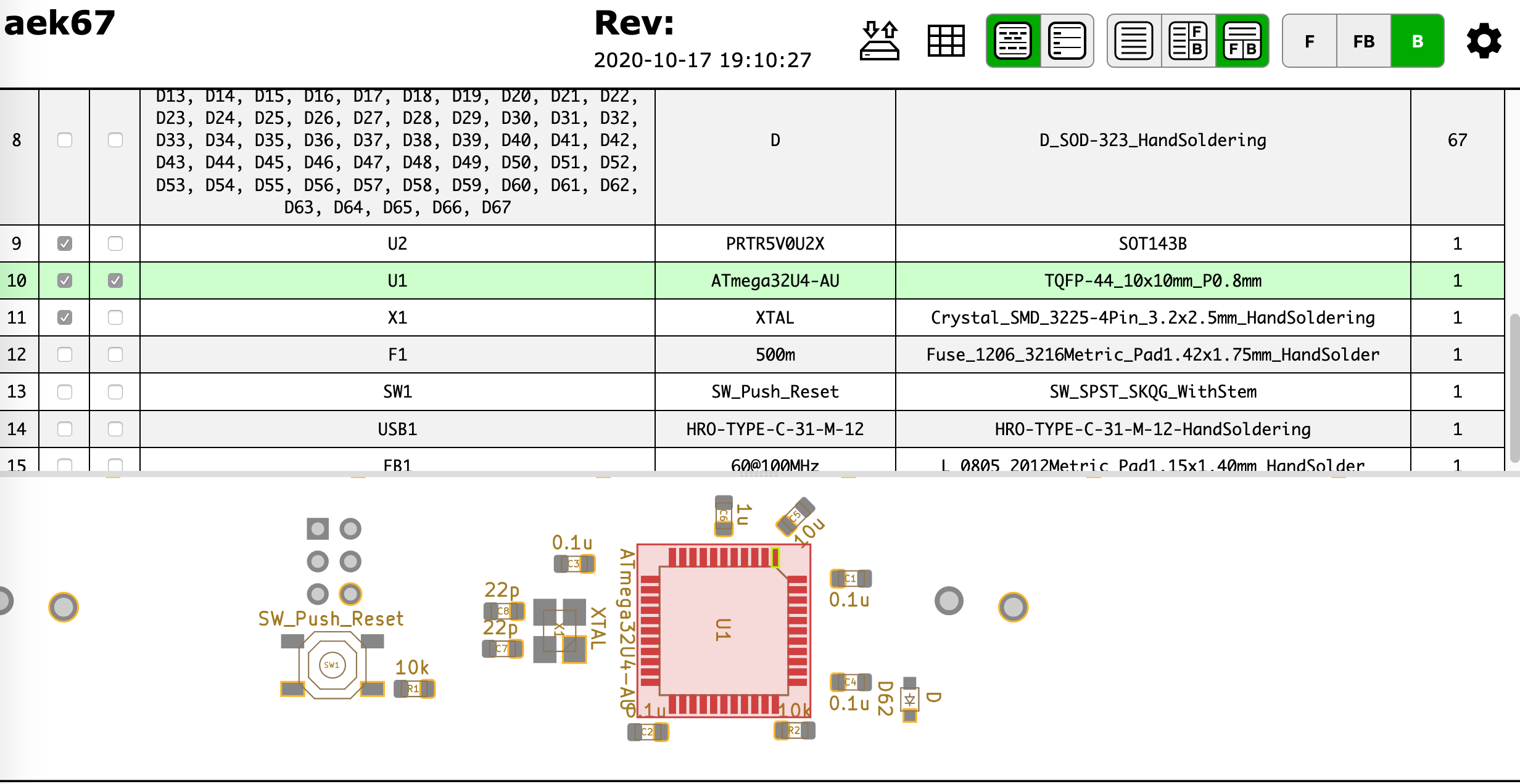
To make sure I’m soldering the component at the right place, I can use the Interactive HTML BOM plugin for Kicad. In the Kicad PCB editor, the plugin can be launched with Tools → External Plugins… → Generate Interactive HTML BOM. In the HTML Defaults section, it’s a good idea to select Highlight first pin and Layer View → Back only. After pressing Generate BOM, a web browser opens containing:

Interactive HTML BOM

Notice that I selected the MCU. I can then see where the first pin is (it is outlined in flashy green), and how the MCU should be oriented.

So, I first add a bit of solder on pad 1 (top right in the picture) and another opposite pad:

Adding solder on some pads

Then I carefully place the MCU and reflow those pads to secure the MCU on the PCB (in the following picture it’s not that well placed, but I didn’t had a better picture):

Securing the MCU

The next step is to add flux on the pins:

Adding flux

And drag soldering the left side:

Drag soldering one side

Repeat the operation on the other three sides. Here’s a picture after soldering the whole component, but before cleaning the flux residues:

MCU soldering result

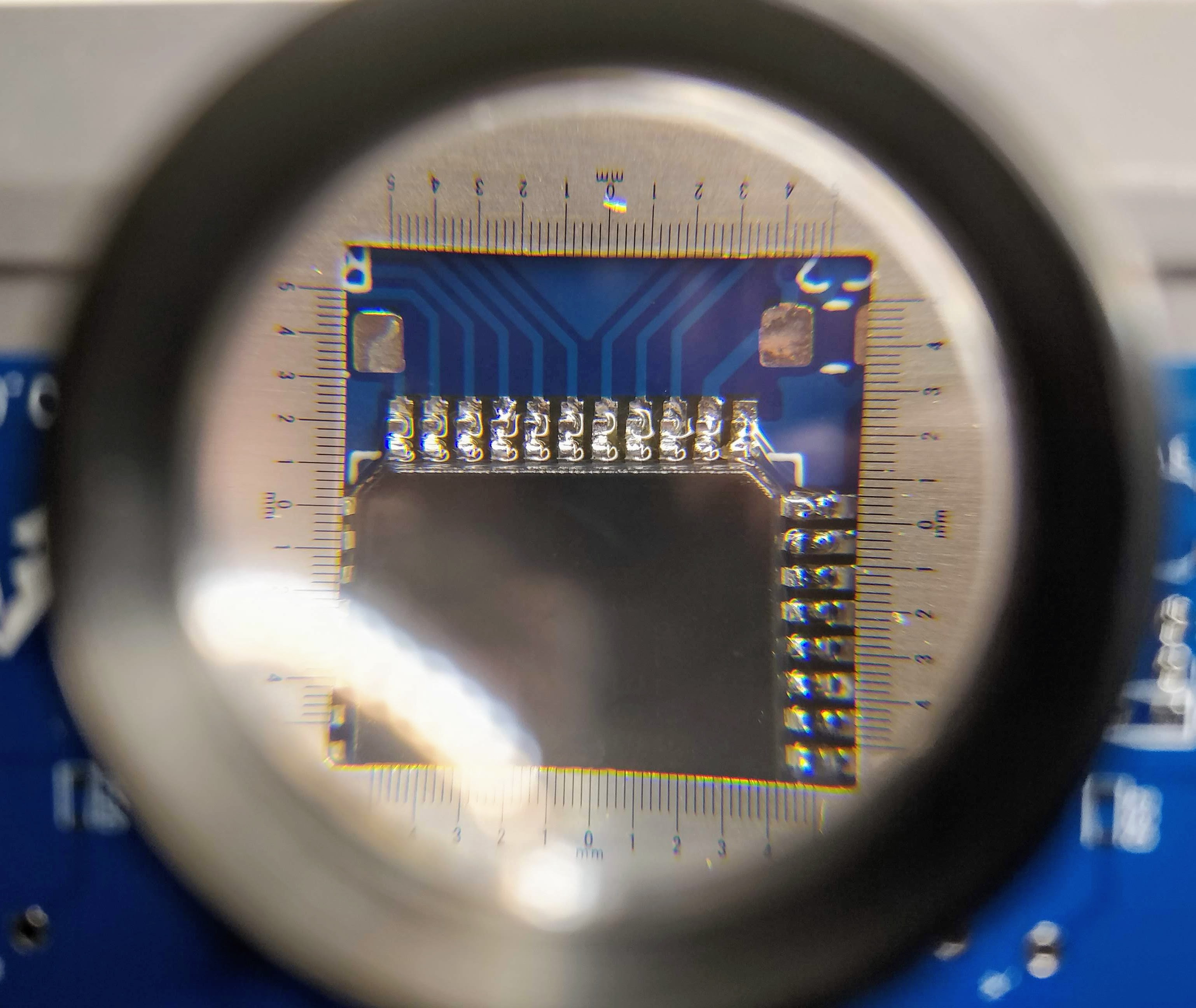
And a visual inspection with the magnifying glass:

Visual inspection

So what to solder next:

  • the crystal oscillator: it’s relatively easy as the pads are gigantic compared to the component size. Note that this component is not polarized (even though there’s a slant in one of the pin, it just shows where pin 1 is).
  • the PRTR5V0U2X and its four pins
  • all decoupling capacitors close to the MCU
  • all resistors
  • the PTC fuse F1
  • the ferrite bead
  • the reset switch

Do not solder the diodes yet. It’s long and tedious, so it’s better to test the MCU works correctly before soldering them.

An advice when soldering is to sort the component bags in the order of the component you want to solder (following the interactive HTML BOM for instance). It’s very hard when looking at SMD components to identity them. Most of the time there’s nothing written on them, or if there’s something it’s not very helpful. That’s why I recommend to open the bag of the component that will be soldered only at the moment of soldering them. So the ritual is:

  • open the bag
  • tear apart the band to release the exact number of needed components
  • place them in a small recipient (so it’s convenient to get them with the tweezers).
  • close the bag
  • solder the components one by one
  • move to the next ones

An alternative is to glue short sections of the components tapes on a cardboard board and tear apart the top tape when needed, then pick the components when ready to solder them.

Once all of the previously mentioned components have been soldered, it’s possible to test the PCB. Warning: do not connect yet the PCB to a computer. There could be a short circuit somewhere that could harm either the host or the keyboard (even though the host have some protections against those kind of failures).

Let’s see how to test the PCB with a multimeter. The first thing to check, is whether there’s continuity between the Vcc path, from the USB Vcc pins to the different MCU pins. If all Vcc pins are correct, check the GND pins. When all are correct, check there’s no continuity between GND and Vcc (at any point on the IC pins and USB pins). If that’s again fine, the next check is to make sure there’s no continuity between D+ and D- (this can be done at the USB connector).

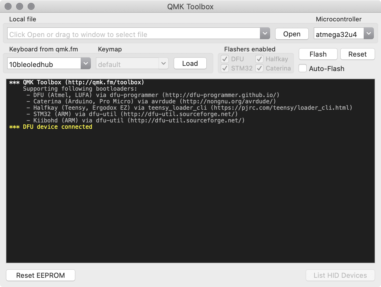
If everything is in oder, it is relatively safe to connect the PCB to a computer. Get an usb cable, then launch QMK toolbox. QMK Toolbox is a simple tool to help flashing QMK on a PCB. Once the keyboard is connected QMK Toolbox should display a yellow line indicating “DFU device connected” (at least for a DFU enabled MCU like our AtMega32U4):

QMK Toolbox

If the test is conclusive, it’s time to solder the 67 diodes. Warning: diodes are polarized components, they need to be soldered with the correct orientation. A diode symbol looks like this:

Diode symbol

One mnemotechnic way to remember which pin is what for a diode is to notice that the vertical bar and triangle form an inverted K and thus is the cathode, the triangle itself looks like an A (so is the anode).

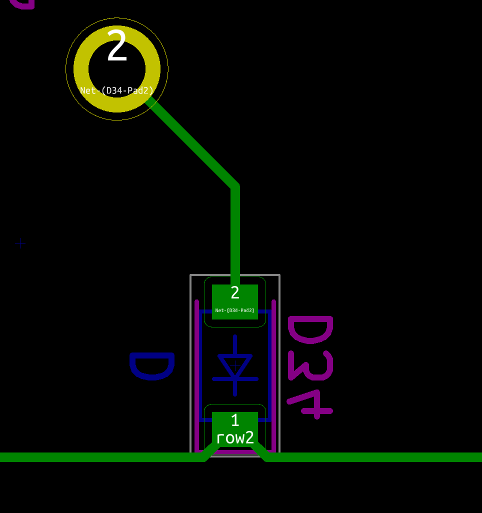
On our schema and PCB, I’ve placed the cathode facing down:

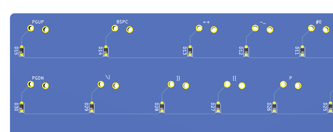
Diode on the PCB

In Kicad, it’s easy to see the orientation of the diode because the B.Fab layer shows how to place it. On the manufactured PCB itself it’s not so easy as the fabrication layer is not shown. Instead we have a small horizontal bar to remind us where the cathode should be placed.

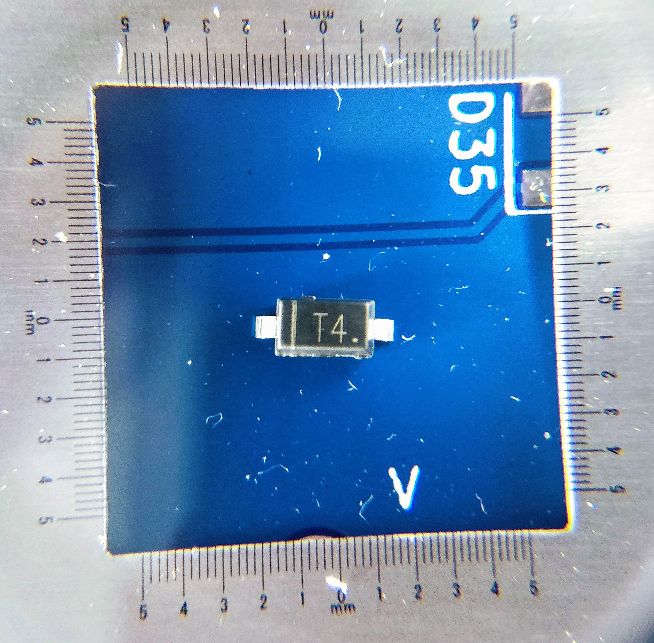
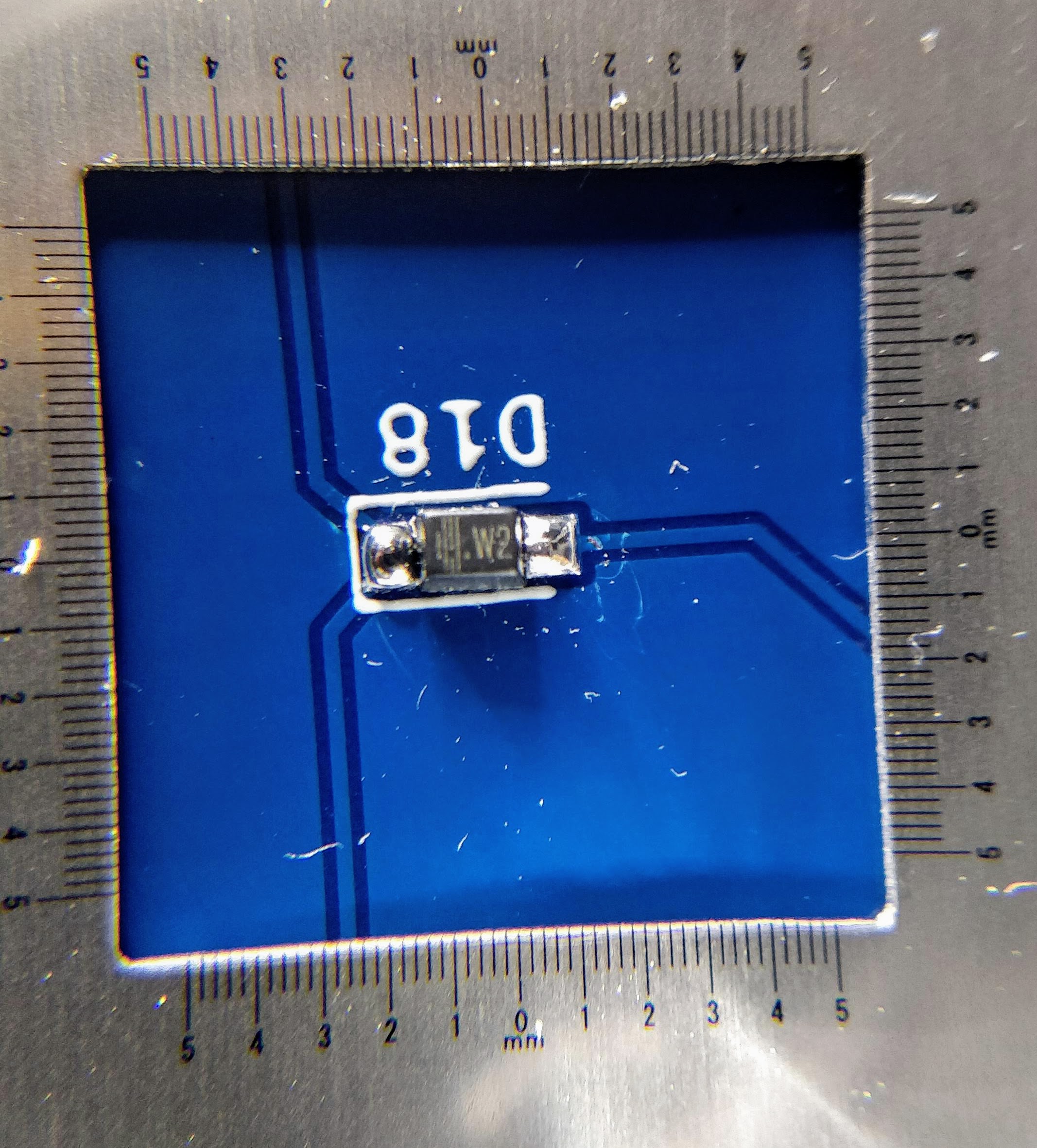
Hopefully the component itself also has a small bar printed on the top (here a close up of a 1N4148W-TP SOD-123, cathode on the left):

SMD diode

So to properly solder those diodes, it’s enough to align the component small bar with the bar printed on the PCB (which can partially be seen for the D35 diode in the image above).

The technique to solder a diode is the same as soldering any two pins SMD components. First add flux on both pads, add a small drop of solder on one of the pad, reflow it while holding the diode, then once solidified add a very small drop of solder on the other pad. Repeat for the 66 other diodes.

Here’s a soldered SOD-323 diode (smaller than the SOD-123 type we choose in this series of articles) :

soldered SMD diode

Once all the diodes are soldered, we can also check with the multimeter that they’re correctly placed and soldered. Again, if I put the multimeter in “diode testing” mode, put the red probe on the switch pin connected to the diode and the black probe on the MCU pin where the row is connected, the multimeter should display a diode forward voltage drop (around 650 mV). If it doesn’t then either the diode is placed in the wrong orientation or there’s a joint issue (that’s how I detected that I had inverted the diode for the P key). If that happens, you need to visually inspect the diode and joints.

Programming the keyboard

To program the controller we’ll use QMK. This is an open source keyboard firmware forked and enhanced from TMK. It supports a miriad of custom keyboards and MCU (including various ATmega and ARM micro-controllers).

Follow QMK setup to install QMK and the needed toolchain on your computer.

Once done, check that you can compile a firmware, for instance the default DZ60 keymap:

% make dz60:default
QMK Firmware 0.11.1

Making dz60 with keymap default

avr-gcc (Homebrew AVR GCC 9.3.0) 9.3.0
Copyright (C) 2019 Free Software Foundation, Inc.
This is free software; see the source for copying conditions.  There is NO
warranty; not even for MERCHANTABILITY or FITNESS FOR A PARTICULAR PURPOSE.

Size before:
   text	   data	    bss	    dec	    hex	filename
      0	  23970	      0	  23970	   5da2	.build/dz60_default.hex

Compiling: keyboards/dz60/dz60.c                                                                    [OK]
Compiling: keyboards/dz60/keymaps/default/keymap.c                                                  [OK]
Compiling: quantum/quantum.c                                                                        [OK]
Compiling: quantum/led.c                                                                            [OK]
Compiling: quantum/keymap_common.c                                                                  [OK]
...
Compiling: lib/lufa/LUFA/Drivers/USB/Core/AVR8/USBController_AVR8.c                                 [OK]
Compiling: lib/lufa/LUFA/Drivers/USB/Core/AVR8/USBInterrupt_AVR8.c                                  [OK]
Compiling: lib/lufa/LUFA/Drivers/USB/Core/ConfigDescriptors.c                                       [OK]
Compiling: lib/lufa/LUFA/Drivers/USB/Core/DeviceStandardReq.c                                       [OK]
Compiling: lib/lufa/LUFA/Drivers/USB/Core/Events.c                                                  [OK]
Compiling: lib/lufa/LUFA/Drivers/USB/Core/HostStandardReq.c                                         [OK]
Compiling: lib/lufa/LUFA/Drivers/USB/Core/USBTask.c                                                 [OK]
Linking: .build/dz60_default.elf                                                                    [OK]
Creating load file for flashing: .build/dz60_default.hex                                            [OK]
Copying dz60_default.hex to qmk_firmware folder                                                     [OK]
Checking file size of dz60_default.hex                                                              [OK]
 * The firmware size is fine - 23816/28672 (83%, 4856 bytes free)
  5.37s user 4.17s system 82% cpu 11.514 total

You should obtain the dz60_default.hex file. You can remove it, it’s not needed.

QMK supports many keyboards and many layouts (called keymaps in QMK) for a given keyboard. A keyboard is defined by a directory in the keyboards/ folder, and each keymap is also a directory in the keymaps/ folder of a keyboard. To build such keymap, one need to use the make <project>:<keyboard>:<keymap> command.

The make command produces a hex file that can be flashed on the controller with QMK Toolbox, which is the recommended method. It is possible to flash from the command line depending on the controller bootloader type. I recommend QMK Toolbox because it is able to autodetect the correct bootloader, check the file size and so on. QMK Toolbox also acts as a console for the controller allowing to see debug statements.

Let’s bootstrap our new keyboard. Hopefully there’s a qmk command to do that:

% ./util/new_keyboard.sh
Generating a new QMK keyboard directory

Keyboard Name: masterzen/aek67
Keyboard Type [avr]:
Your Name: masterzen

Copying base template files... done
Copying avr template files... done
Renaming keyboard files... done
Replacing %YEAR% with 2020... done
Replacing %KEYBOARD% with aek67... done
Replacing %YOUR_NAME% with masterzen... done

Created a new keyboard called masterzen/aek67.

To start working on things, cd into keyboards/masterzen/aek67,
or open the directory in your favourite text editor.

This creates a set of files in keyboards/masterzen/aek67 that contains the default configuration for an AVR (ie AtMega) keyboard, including the default keymap:

% find keyboards/masterzen/aek67
keyboards/masterzen/aek67
keyboards/masterzen/aek67/aek67.h
keyboards/masterzen/aek67/config.h
keyboards/masterzen/aek67/keymaps
keyboards/masterzen/aek67/keymaps/default
keyboards/masterzen/aek67/keymaps/default/keymap.c
keyboards/masterzen/aek67/keymaps/default/readme.md
keyboards/masterzen/aek67/readme.md
keyboards/masterzen/aek67/aek67.c
keyboards/masterzen/aek67/info.json
keyboards/masterzen/aek67/rules.mk

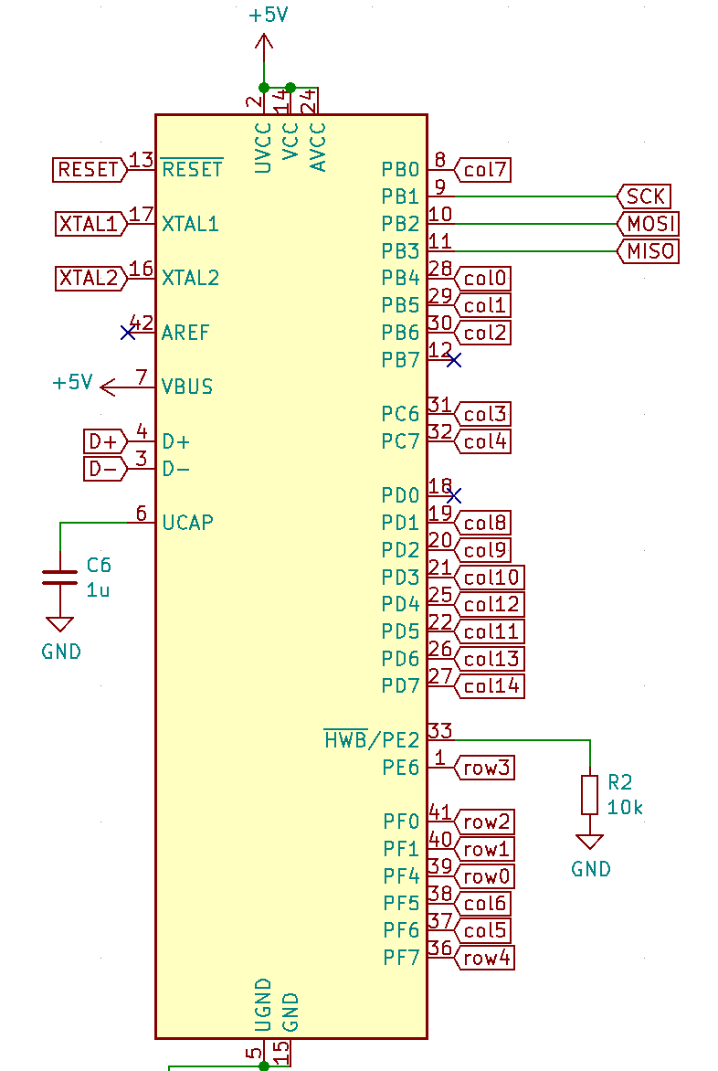
I need to edit those files to map the hardware and matrix I created. Let’s start with the config.h file. This file contains the matrix description for this keyboard. We need to explain to QMK, what columns map to what pins on the MCU, and the orientation of the diodes. Based on our electronic schema, I can just write down the list of rows pins and columns pins:

MCU pins assignment

Here’s an extract of our config.h:

/* key matrix size */
#define MATRIX_ROWS 5
#define MATRIX_COLS 15

/*
 * Keyboard Matrix Assignments
 */
#define MATRIX_ROW_PINS { F4, F1, F0, E6, F7 }
#define MATRIX_COL_PINS { B4, B5, B6, C6, C7, F6, F5, B0, D1, D2, D3, D5, D4, D6, D7 }
#define UNUSED_PINS { B7, D0 }

/* COL2ROW, ROW2COL */
#define DIODE_DIRECTION COL2ROW

I defined here that the matrix is 5x15, and the ports of the rows and columns (in increasing order). Also, I tell QMK that the diodes are hooked between the columns and the rows (ie cathodes connected to the rows).

Next in rules.mk, we tell QMK everything about the controller used in this keyboard (there’s no need to edit anything there):

# MCU name
MCU = atmega32u4

# Bootloader selection
BOOTLOADER = atmel-dfu

# Build Options
#   change yes to no to disable
#
BOOTMAGIC_ENABLE = lite     # Virtual DIP switch configuration
MOUSEKEY_ENABLE = yes       # Mouse keys
EXTRAKEY_ENABLE = yes       # Audio control and System control
CONSOLE_ENABLE = no         # Console for debug
COMMAND_ENABLE = no         # Commands for debug and configuration
# Do not enable SLEEP_LED_ENABLE. it uses the same timer as BACKLIGHT_ENABLE
SLEEP_LED_ENABLE = no       # Breathing sleep LED during USB suspend
# if this doesn't work, see here: https://github.com/tmk/tmk_keyboard/wiki/FAQ#nkro-doesnt-work
NKRO_ENABLE = no            # USB Nkey Rollover
BACKLIGHT_ENABLE = no       # Enable keyboard backlight functionality
RGBLIGHT_ENABLE = no        # Enable keyboard RGB underglow
BLUETOOTH_ENABLE = no       # Enable Bluetooth
AUDIO_ENABLE = no           # Audio output

The next step is to define a key to matrix position mapping in aek67.h so that writing our keymap will be a bit easier:

...
#define LAYOUT_67_ansi( \
	K000, K001, K002, K003, K004, K005, K006, K007, K008, K009, K010, K011, K012, K013, K014, \
	K100, K101, K102, K103, K104, K105, K106, K107, K108, K109, K110, K111, K112, K113, K114, \
	K200, K201, K202, K203, K204, K205, K206, K207, K208, K209, K210, K211,       K213, K214, \
	K300, K301, K302, K303, K304, K305, K306, K307, K308, K309, K310,       K312, K313, K314, \
	K400, K401, K402,                   K406,                   K410, K411, K412, K413, K414  \
) { \
	{ K000,  K001,  K002,  K003,  K004,  K005,  K006,  K007,  K008,  K009,  K010,  K011,  K012,  K013,  K014 }, \
	{ K100,  K101,  K102,  K103,  K104,  K105,  K106,  K107,  K108,  K109,  K110,  K111,  K112,  K113,  K114 }, \
	{ K200,  K201,  K202,  K203,  K204,  K205,  K206,  K207,  K208,  K209,  K210,  K211,  KC_NO, K213,  K214 }, \
	{ K300,  K301,  K302,  K303,  K304,  K305,  K306,  K307,  K308,  K309,  K310,  KC_NO, K312,  K313,  K314 }, \
	{ K400,  K401,  K402,  KC_NO, KC_NO, KC_NO, K406,  KC_NO, KC_NO, KC_NO, K410,  K411,  K412,  K413,  K414 }  \
}

So the C macro LAYOUT_67_ansi contains 67 entries, one for each key, named by their rows and columns number (ie K204 is row2 and col4). This maps to a structure that represents the matrix in QMK (a double dimension array or rows and columns). Where the physical matrix has no switches (for instance in the bottom row before and after K406), we assign KC_NO so that QMK knows there’s nothing to be found there.

Next, let’s create the keymap. The keymap represents a mapping between the matrix switches and their functionality. When pressing a key, QMK will lookup in the keymap what keycode to send back to the computer. The computer will then interpret this keycode to a real character in function of the chosen layout. The keycode are defined by the USB HID standard. In QMK, they are defined as C macro whose name start with KC_. For instance KC_Q is the keycode for the Q key. See the QMK keycode table for an exhaustive list.

In QMK a keymap is a double dimension array of MATRIX_ROWS rows and MATRIX_COLS columns.

But that’s not the end of the story. QMK exposes different keymap layers. Layers are ways to assign multiple functions to a single key. We can assign a key in our keymap to switch to another layer where the keycode assigned is different than in the base layer. This is used for instance to map the function keys (F1 to F10) to the number keys.

Here’s the content of default/keymap.c:

enum layers {
    BASE,  // qwerty
    _FL,   // function key layer
};

/*
 * ,---------------------------------------------------------------------|
 * |`  |1  |2  |3  |4  |5  |6  |7  |8  |9  |0   |-   |=  |Backspace| PgUp|
 * |---------------------------------------------------------------------|
 * |Tab  |Q  |W  |E  |R  |T  |Y  |U  |I  |O  |P  |[  | ]  |   \     |PgDn|
 * |---------------------------------------------------------------------|
 * |Caps  |A  |S  |D  |F  |G  |H  |J  |K  |L  |;  |'  |  Enter     | Ins |
 * |---------------------------------------------------------------------|
 * |Shft    |Z  |X  |C  |V  |B  |N  |M  |,  |.  |/  |Shift       |Up| Del|
 * |---------------------------------------------------------------------|
 * |Ctrl|GUI |Alt |     Space                    |Alt |Fn  |  Lt |Dn |Rt |
 * `---------------------------------------------------------------------|'
 */
const uint16_t PROGMEM keymaps[][MATRIX_ROWS][MATRIX_COLS] = {
    [BASE] = LAYOUT_67_ansi(
        KC_ESC, KC_1,   KC_2,  KC_3,  KC_4,  KC_5,  KC_6,  KC_7,  KC_8,  KC_9,  KC_0,    KC_MINS,  KC_EQL,  KC_BSPC, KC_PGUP,
        KC_TAB, KC_Q,   KC_W,  KC_E,  KC_R,  KC_T,  KC_Y,  KC_U,  KC_I,  KC_O,  KC_P,    KC_LBRC,  KC_RBRC, KC_BSLS, KC_PGDN,
        KC_CAPS, KC_A,  KC_S,  KC_D,  KC_F,  KC_G,  KC_H,  KC_J,  KC_K,  KC_L,  KC_SCLN, KC_QUOT,           KC_ENT,  KC_INS,
        KC_LSFT, KC_Z,  KC_X,  KC_C,  KC_V,  KC_B,  KC_N,  KC_M, KC_COMM, KC_DOT,KC_SLSH,          KC_RSFT, KC_UP,   KC_DEL,
        KC_LCTL, KC_LGUI, KC_LALT,                  KC_SPC,                      KC_RALT, MO(_FL), KC_LEFT, KC_DOWN, KC_RGHT),

    [_FL] = LAYOUT_67_ansi(
        KC_GRV,  KC_F1, KC_F2, KC_F3, KC_F4, KC_F5, KC_F6, KC_F7, KC_F8,  KC_F9, KC_F10, KC_F11, KC_F12, KC_DEL, RESET,
        _______, _______, _______, _______, _______, _______, _______, _______, _______, _______, _______, _______, _______, _______, KC_HOME,
        _______, _______, _______, _______, _______, _______, _______, _______, _______, _______, _______, _______, _______, KC_END,
        _______, _______, _______, _______, _______, _______, _______, _______, _______, _______, _______, _______, KC_VOLU,_______,
        _______, _______, _______,                   _______,                            _______, MO(_FL), KC_BRID, KC_VOLD, KC_BRIU),
};

Notice a few things:

  • I’m using the LAYOUT_67_ansi macro that I defined in aek67.h. This is to simplify using the matrix, because the matrix doesn’t have all the switches implemented.
  • there are two layers, the base one called BASE and the so-called function layer _FL, that contains a few more keys.
  • the _______ is an alias for KC_TRANS which means that this key isn’t defined in this layer. When pressing this key while being in this layer, the keycode that will be emitted is the first one to not be KC_TRANS in the layer stack. That means that Enter for instance is still Enter even for the _FL layer, but the up arrow key is volume up in the _FL layer.
  • I’m including a RESET key, so that it is easy to enter DFU mode to flash the keyboard (no need to open the case to get access to the hardware reset button)
  • MO(_FL) is a special keycode that tells QMK to momentary switch to the _FL layer as long as the key id pressed. So activating RESET means maintaining MO(_FL) key and pressing the Page up key.

Now let’s build the firmware:

% make masterzen/aek67:default
QMK Firmware 0.11.1

Making masterzen/aek67 with keymap default

avr-gcc (Homebrew AVR GCC 9.3.0) 9.3.0
Copyright (C) 2019 Free Software Foundation, Inc.
This is free software; see the source for copying conditions.  There is NO
warranty; not even for MERCHANTABILITY or FITNESS FOR A PARTICULAR PURPOSE.

Size before:
   text	   data	    bss	    dec	    hex	filename
      0	  18590	      0	  18590	   489e	.build/masterzen_aek67_default.hex

Compiling: keyboards/masterzen/aek67/aek67.c                                                        [OK]
Compiling: keyboards/masterzen/aek67/keymaps/default/keymap.c                                       [OK]
Compiling: quantum/quantum.c                                                                        [OK]
Compiling: quantum/led.c                                                                            [OK]
Compiling: quantum/keymap_common.c                                                                  [OK]
Compiling: quantum/keycode_config.c                                                                 [OK]
Compiling: quantum/matrix_common.c                                                                  [OK]
Compiling: quantum/matrix.c                                                                         [OK]
Compiling: quantum/debounce/sym_defer_g.c                                                           [OK]
...
Compiling: lib/lufa/LUFA/Drivers/USB/Core/AVR8/USBController_AVR8.c                                 [OK]
Compiling: lib/lufa/LUFA/Drivers/USB/Core/AVR8/USBInterrupt_AVR8.c                                  [OK]
Compiling: lib/lufa/LUFA/Drivers/USB/Core/ConfigDescriptors.c                                       [OK]
Compiling: lib/lufa/LUFA/Drivers/USB/Core/DeviceStandardReq.c                                       [OK]
Compiling: lib/lufa/LUFA/Drivers/USB/Core/Events.c                                                  [OK]
Compiling: lib/lufa/LUFA/Drivers/USB/Core/HostStandardReq.c                                         [OK]
Compiling: lib/lufa/LUFA/Drivers/USB/Core/USBTask.c                                                 [OK]
Linking: .build/masterzen_aek67_default.elf                                                         [OK]
Creating load file for flashing: .build/masterzen_aek67_default.hex                                 [OK]
Copying masterzen_aek67_default.hex to qmk_firmware folder                                          [OK]
Checking file size of masterzen_aek67_default.hex                                                   [OK]
 * The firmware size is fine - 16028/28672 (55%, 12644 bytes free)
  3.87s user 3.19s system 96% cpu 7.308 total

If it doesn’t compile, fix the error (usually this is a bad layer mapping, missing a comma, etc), and try again. The resulting firmware will be in masterzen_aek67_default.hex file at the QMK root.

To properly finish the work, I also need to build a QMK Configurator json description file. This file tells the QMK Configurator how the keyboard looks (ie its layout) so it can display correctly the keyboard. It’s for people that don’t want to create their keymap in C like I did here. Producing this json file is easy to do from the Keyboard Layout Editor. Just copy the KLE raw content to a .txt file and run:

% qmk kle2json aek67-kle.txt
Ψ Wrote out info.json

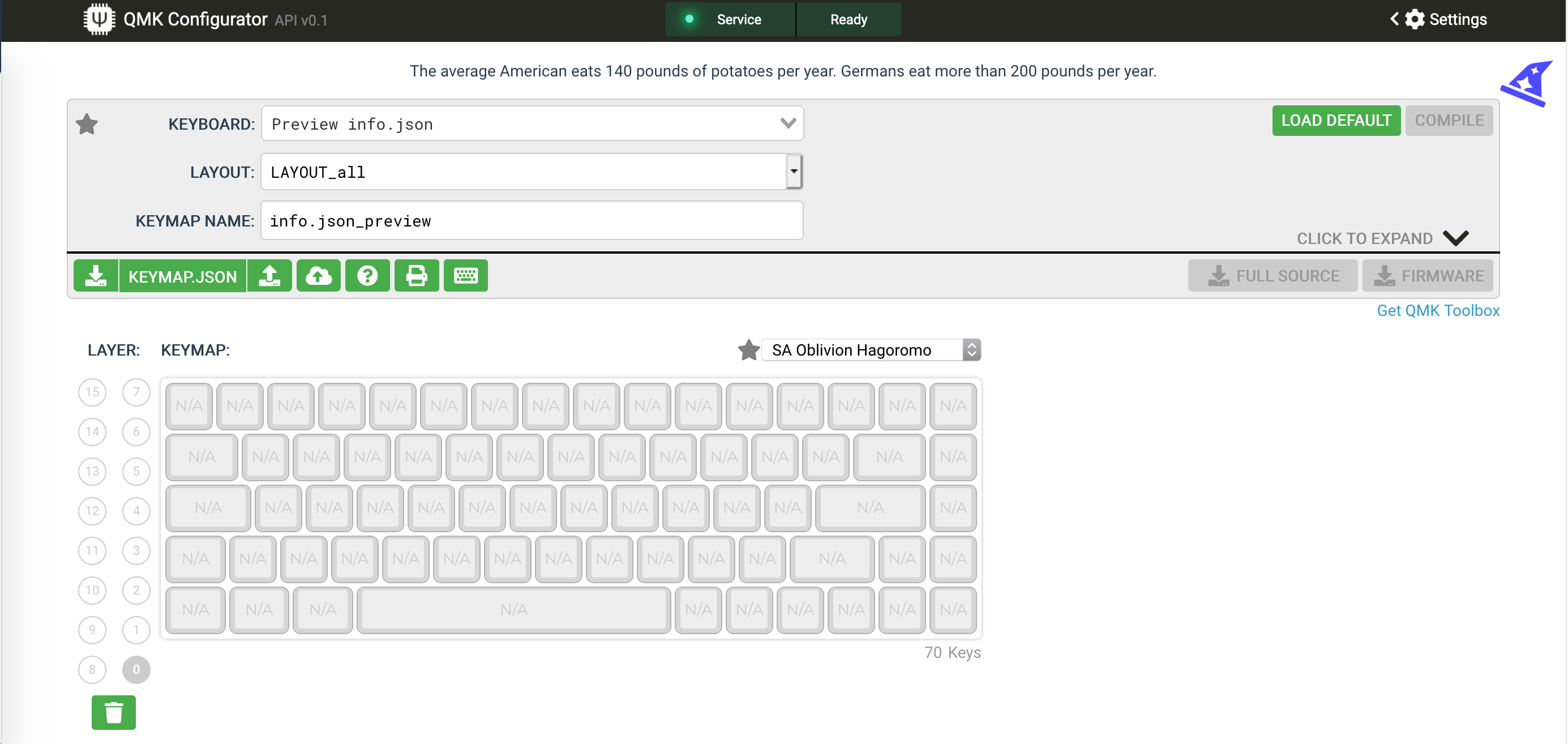
It is possible to try the info.json file by going to the QMK Configurator and enter the Preview Mode by pressing Ctrl+Shift+i. This brings up a file selector window in which it is possible to open our info.json. If all goes well, the configurator will display the keyboard layout without any key label:

QMK Configurator

Finally, I can try to flash the firmware to the PCB:

  1. Connect the PCB to the computer
  2. Open QMK Toolbox
  3. Press the Keyboard reset button (if not already in DFU mode)
  4. QMK Toolbox will notice a DFU keyboard is connected by displaying *** Atmel DFU device connected
  5. Load the firmware that was just built
  6. Choose the ATMega32U4 microcontroller
  7. Press the flash button

You should see something like this:

*** Attempting to flash, please don't remove device
>>> dfu-programmer atmega32u4 erase --force
    Erasing flash...  Success
    Checking memory from 0x0 to 0x6FFF...  Empty.
>>> dfu-programmer atmega32u4 flash --force /path/to/qmk_firmware/masterzen_aek67_default.hex
    0%                            100%  Programming 0x3F00 bytes...
    [>>>>>>>>>>>>>>>>>>>>>>>>>>>>>>>>]  Success
    0%                            100%  Reading 0x7000 bytes...
    [>>>>>>>>>>>>>>>>>>>>>>>>>>>>>>>>]  Success
    Validating...  Success
    0x3F00 bytes written into 0x7000 bytes memory (56.25%).
>>> dfu-programmer atmega32u4 reset
*** AtmelDFU device disconnected

At this point your computer should recognize that a new keyboard has been connected. If you press any switches it should produce a letter.

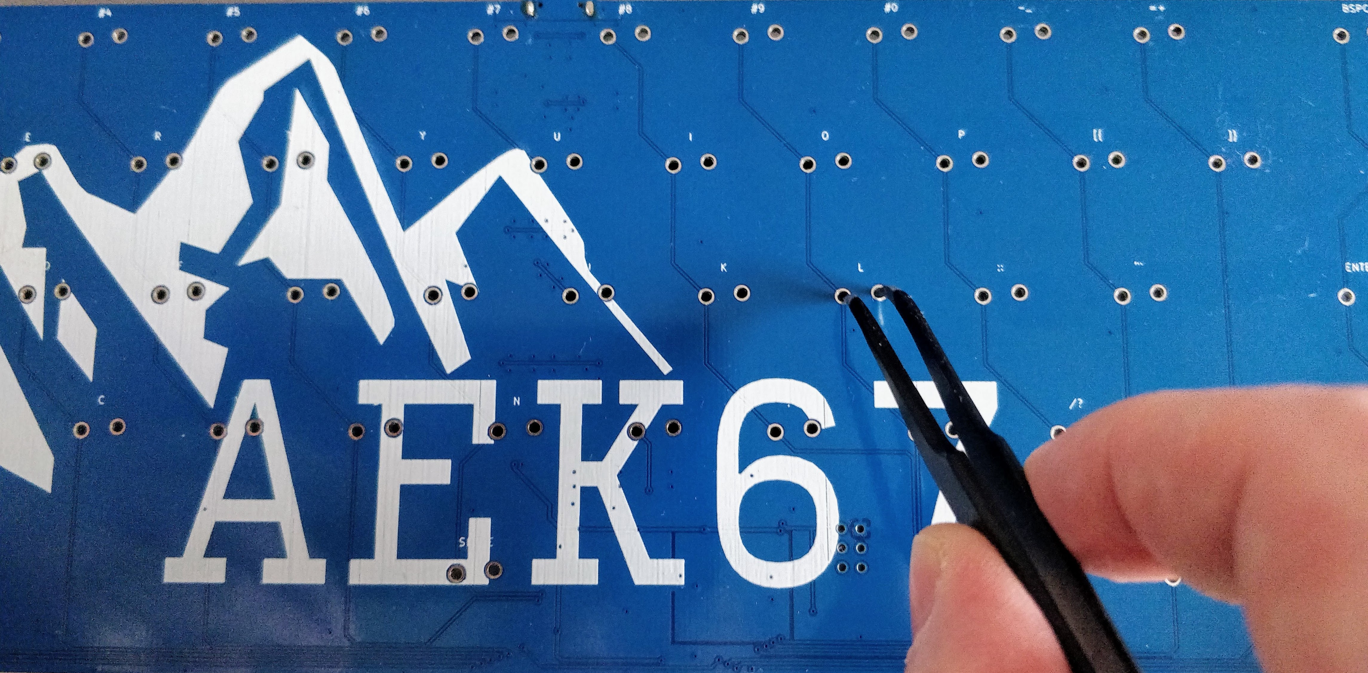
You can now test the keyboard and the keymap with the QMK Keyboard Tester. To do so, while the PCB is connected to the computer, use the tweezer to make contact between the two pins of each switch:

Testing with Tweezers

If the PCB and keymap are working correctly, the keyboard tester should display the key as registered:

QMK Tester

And voila, I now have a fully functional keyboard PCB!

What’s cooking next

And I think that episode concludes the series about keyboard PCB. I’ll expand soon the series of posts to talk about designing a nice case for the PCB.

I hope to be able to cover at least the following:

  • plate design
  • case design
  • selecting screws and nuts
  • 3D renders
  • technical plans
  • fabrication
  • prototype assembly

Thanks for following, and stay tuned for the next episodes!
Designing a keyboard from scratch - Part 3

33 minute read

Welcome for the third episode of this series of posts about designing a full fledged keyboard from scratch. The first episode focused on the electronic schema of the keyboard controller, the second one was on the components’ layout. In this one I’ll cover:

  • how to route the matrix
  • the MCU
  • the USB datalines
  • adding drawings on the soldermask

This is a long episode that took me a quite long time to produce. Feel free to leave a comment if you have any questions or find anything suspect :)

The Art of Routing

Routing is the process of connecting the various pins and pads of the circuits with copper traces while respecting the electronic schema. There are things that can and can’t be done for the PCB to be functional, for instance circuits have specific constraints for EMI, impedance matching, etc.

In the previous episode I decided to use a two layers PCB (which is the best compromise between cost and ease of routing for such projects). The switches are placed on the front layer, and because they are through-hole components they are being soldered on the back. All the rest of the components are laid out on the back of the board.

In the part 2 of this series of posts, I shown how to design the matrix schema. The matrix is a set of non-intersecting rows and columns. This means that if we were to route the matrix on the same PCB face we’d had an issue: all rows would collide with the columns.

Hopefully, since there are two layers in this PCB, I can route the columns on one side and the rows on the other side. Unfortunately there are other components to connect: the USB Type-C connector (and its ESD protection circuits), the MCU, the reset push-button, etc.

The USB Type-C connector is on the back layer at the top of the board, the MCU is also on the back layer but at the bottom. That means there are a few tracks to route vertically akin to the columns.

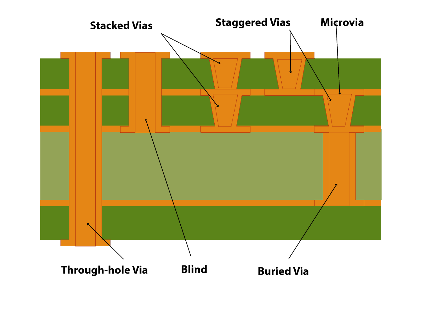
Inevitably some traces will intersect other traces. In such case it is possible to switch the trace to another layer by placing a via. A via is an electrical connection between two layers. The trace can then extend from one layer to another. Basically it is a hole that is metal plated to be able to conduct electricity. Note that there are different kinds of via, depending on if they cross the whole board or only some layers. In the case of two layers PCB, it will be through-hole vias.

All Vias types

With a pair of vias in series the trace can jump to the other side and come back to its original side.

Another important thing to know is that a through hole pad (like the switch ones, but this is valid for any through-hole components) is available on both layers. This means a trace can piggy-back a switch pad to switch layer:

TH Pad to switch layer

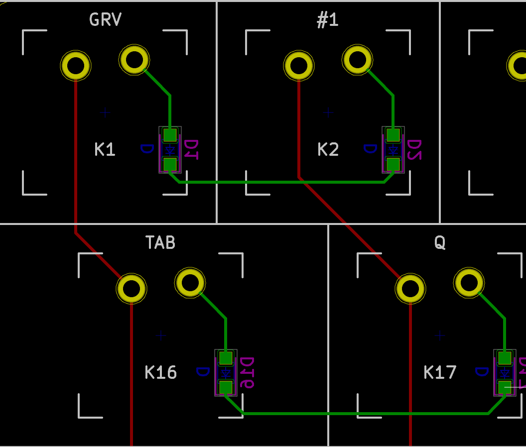
To prevent via abuse, the routing needs to take advantage of the number of layers. So for instance I can route the columns on the front layer, and the rows on the back layer.

Routing columns on front

But it is also possible to do the reverse:

Routing columns on back

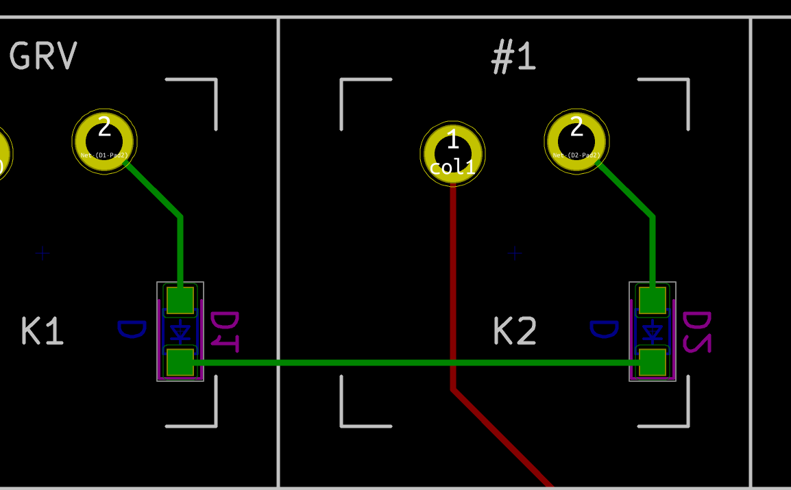
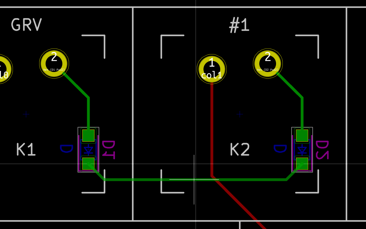
I was forced to use vias to jump other the column col1, because the diodes are on the backside. I tried two possibilities, using vias only for the minimal jump or using vias on the pad. Notice how both seems inelegant. Putting a via on a pad is also not a good idea unless the manufacturer knows how to do plugged vias. This can be needed for some high-frequency circuits where the inductance needs to be reduced. This isn’t the case of this very low speed keyboard, so I’ll refrain doing this.

Routing matrix columns

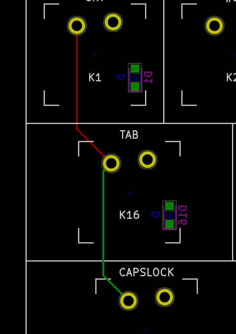
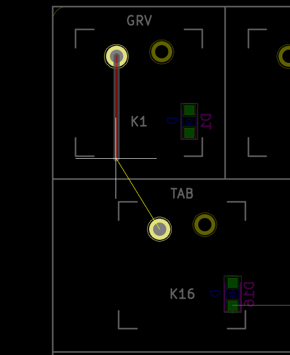
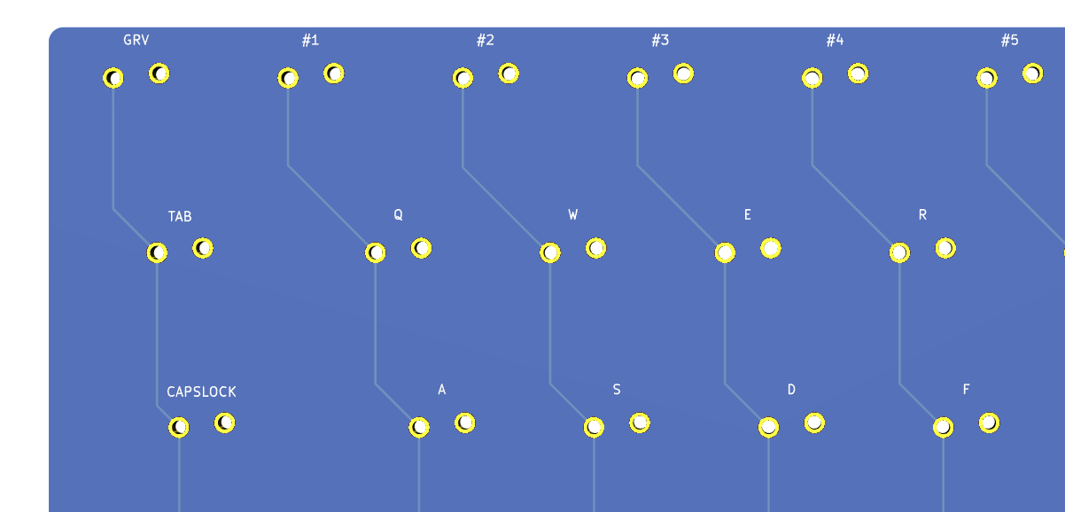
Let’s route the columns. Start from the top left switch (or any other switch), then activate trace routing by pressing the x shortcut. Make sure that the F.Cu layer is active. If it’s not the case, you can switch from one layer to another by pressing the v shortcut. Caution: if you press v while routing a track, a via will be created. To start routing, click on the GRV left pad, then move the mouse down toward the TAB switch left pad (follow the net yellow highlighted line which shows where the net is connected):

Routing first column

Notice that while routing a specific net, this one is highlighted in yellow, along with the pads that needs to be connected.

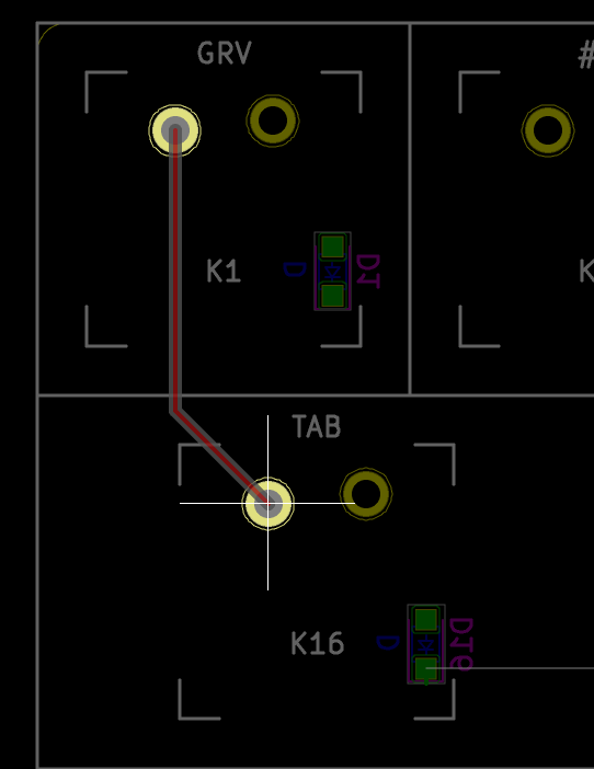
Keep going until you reach the next pad, and then click to finish the trace. Notice that the route is automatically bent and oriented properly. This is the automated routing:

Routing 2nd step

Keep going until all columns have been routed. Sometimes the trace is not ideally auto-routed by the automated routing system. In this case, it is possible to fix the problem by selecting the segment and use the Drag Track Keep Slope (shortcut d) to move the trace. For instance this trace pad connection could be made better :

Not ideally oriented trace

Dragging the track with d until I eliminated the small horizontal trace:

better trace

When all the columns are completed, the PCB looks like this:

All columns routed

Notice that I haven’t connected the columns to the MCU yet, hence all the nets are directly linked to their assigned pads with those white lines.

Using the Show local ratsnest function we can highlight the columns nets, and verify that the connection scheme in part 2 is correct.

The idea was to have the columns on the extreme left or right be assigned the bottom part of the MCU (respectively left and right pads), and the center left columns (col5, col6) the left pads, the center columns col7 a free top pad, and the center right columns col8, col9 the right pads.

This gives this result:

MCU much less mess

But before connecting the columns to the MCU, it’s better to route the USB data-lines and power rails.

USB differential pair

The D+/D- USB data lines form what is called a differential pair. The idea is to send a complement signal on two wires instead of the normal signal on one. Traditionally a component uses GND as the reference for a signal in a single wire. This can be subject to EMI and noise. In a differential pair (and provided the impedance matches on both wire), the noise will affect both wire the same way. Since the MCU computes the difference between the two signals to recover the correct value, the noise is removed (because it is the same on both lines). The differential pair is thus much more immune to EMI and noise than a single trace.

Thus, differential pairs needs to be routed with care. Both trace needs to obey some important rules listed below.

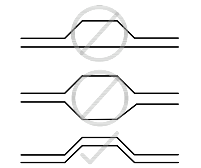
Respect symmetry

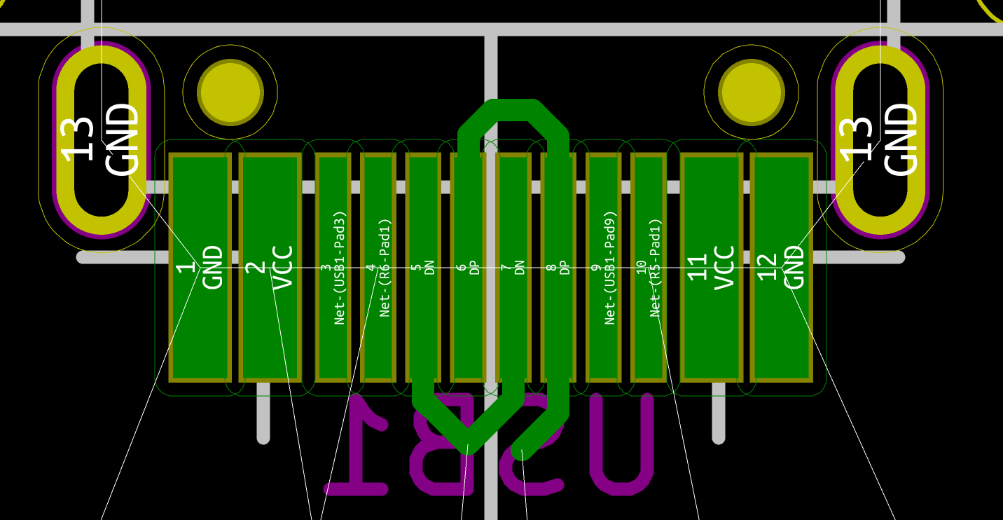
To conserve coupling it’s best for the differential pair traces to keep their symmetry as good as possible.

Keep symmetry Keep symmetry

Match Trace Length

The noise-cancelling advantage of a differential pair works only if both signals arrive at the same time at the endpoint. If the traces have different lengths, one of the signal will arrive a bit later than the other, negating the effect. There’s a tolerance though, especially since this keyboard USB differential pair will run at the USB Full Speed standard (12 Mbit/s).

It’s possible to compute the time difference of the signals in function of the length difference. With the Full Speed standard a few centimeters difference will not incur a difference in arrival time, but this wouldn’t be true with high-speed signals. It’s best to keep the good practice of matching length all the time.

There’s no function in Kicad to check trace length, hopefully the trace length plugin can be used to check both traces length of the pair.

Reduce distance between traces

Obviously this will take less space on the PCB, which is good. But also the differential pair return current will flow in the ground plane below (if there’s one), possibly creating a current loop generating noise, if both tracks are not coupled enough because of their relative distance. This is again less an issue with USB Full Speed signals like the one this keyboard deals with (or with 2 layers boards without ground planes).

Minimize number of vias

Each via adds inductance to the trace. It is usually recommended to not route those differential pairs through vias. But if vias have to be used anyway, make sure to use the same number of vias for both traces of the pair. With USB Full Speed signals, adding a few amounts of vias would probably not be detrimental, but it’s better to keep those traces on the same layer as much as we can as a good habit. Make sure to place all the IC so that there’s no need for differential pairs to change layers. That’s also the reason differential pairs should be routed first.

Spacing around differential pairs

The differential pair should not be too close to other signals or other differential pairs. A good rule of thumb is to apply a spacing of 5 times the trace width (this is known as the 5W rule).

Where the differential pair comes close to high speed signals (for instance clock traces), the spacing must be increased again (for instance 50mils). Differential pairs should also be spaced from other differential pairs to prevent cross-talk (use the same 5W rule).

Watch the Return Current

Spoiler alert: all circuits form a closed loop. The signal in a differential pair is a current that needs to flow back to it’s source at some point. At higher frequencies, the return current will follow the lowest impedance path. This usually happens to be the closest reference plane (a ground or power plane if there’s one). If there’s a void or a split in the reference plane, the return current will have a longer path leading to excess electromagnetic emissions, delayed signal, etc.

Don’t route close to crystals

The differential pairs should not be routed under or near a crystal oscillator or resonator.

Crossing a differential pair

When a single track or another differential pair crosses (on a different layer) a differential pair, do it with an angle of > 30º and < 150º to minimize cross talk. To make it more easy target 90º intersections.

Do not use striplines

A stripline is a layer trace embedded in a dielectric medium itself sandwiched by two copper plane. On the reverse a microstrip is a trace at the surface (not embedded). It’s best to route differential pairs as microstrips.

Striplines vs Microstrip

Avoid Bends

If possible, the differential pair should never do a straight U-turn. When bending, maintain a 135º angle all the time.

Keep away from edges

The recommendation is to keep at least 90mils between the traces and the ground plane edges.

Control the trace impedance

The USB 2.0 standard requires the transmission lines (ie cables and connected PCB tracks) to have a differential impedance of 90 ohms (which translate to a single line impedance of 45 ohms) +- 10%.

Maintaining the impedance is capital to prevent high frequency signals to bounce. To perform controlled impedance routing, you need to compute the single trace width and spacing (there are calculators online and even one in Kicad; the free Saturn PCB calculator is a good reference but works on Windows only).

It’s relatively easy to control the impedance if there’s a continuous ground plane not far below the tracks (so it’s best to route those on 4+ layers PCB). But for a 2-layers PCB, assuming one of the layer is an uninterrupted ground plane, the trace size would have to be 38 mils spaced with 8 mils to match the 90 ohms impedance. This is because the height of the dielectric board is around 1.6 mm for a 2 layers board, whereas it is less than a 1 mm between two copper layers on the same side of the board.

Hopefully, if our traces are shorter than the signal wavelength there’s no need to implement controlled impedance. With a tool like the Saturn PCB Calculator we can estimate the USB Full Speed wavelength and thus our max trace length.

The USB Full Speed rise time is between 4 ns to 20 ns. When injecting the worst case of 4 ns in the Bandwidth & Max Conductor Length calculator, the result is a bit more than 18 cm. Since this keyboard is currently 9.5 cm wide and the USB D+/D- will be traced as straight as possible, the differential pair length will be well within the safety margin. Based on this, I’m going to use 10 mils as trace width and spacing.

Forbid stubs

Stubs should be avoided as they may cause signal reflections. For USB, this is seldom a problem as the data traces are point-to-point.

Want to know more?

Most of these recommendations were gleaned from TI High-SpeedLayoutGuidelines, Silicon Labs USB Hardware Design Guide, Atmel AVR1017: XMEGA - USB Hardware Design Recommendations, Intel EMI Design Guidelines for USB Components. I also recommend reading Eric Bogatin - Signal and Power Integrity - Simplified and Henry W. Ott - Electromagnetic Compatibility Engineering. Refer to those documentations for more information.

Routing

Now let’s apply this knowledge to this keyboard. First I need to prepare the USB connector data lines: since there are 4 pads for the two datalines (to support reversibility) they need to be connected together:

USB datalines connector

Use the RouteDifferential Pairs feature and start laying out the traces from the connector. Uh oh, an error pops-up:

Differential Pair error

To be able to route a differential pair, Kicad requires its nets to obey a specific naming. Net names should end up in P/N or +/-, which is not the case here. The USB pads nets have no name, as they acquire their name only after the impedance matching resistors. To correct this, I just need to assign name to the wires in the schema editor:

Adding names

And finally using Update PCB from schematics, I can start routing the USB data-lines (using the RouteDifferential pair function):

Routing the USB data-lines

The next step is to connect the differential pair to the PRTR5V0U2X. Unfortunately Kicad is not very smart when connecting a differential pair to pads. It’s better to stop drawing the differential pair, switch to single track routing mode and connect the pads to the differential pairs. Since it’s important to minimize stubs, it’s best to uncouple a bit the differential pair to connect it to pads, like this:

PRTR5V0U2X connection

Then, the differential pair can be routed to the pair of impedance matching resistors (which are located close to the MCU):

USB D+/D-

To connect the resistors to the MCU with a differential pair, it’s easier to start from the MCU by using the RouteDifferential Pair function and connect the MCU pads to the resistors pads:

To the MCU

Now, I can check both trace lengths with the Measure Length of Selected Tracks plugins. To do that, select one trace of the pair, and use the u shortcut to select it fully. In the case of this keyboard, I got 70.05 mm for the left traces and 69.90 mm for the right one. This is small enough to not try to optimize it.

The final routing of this differential pair looks like this:

USB D+/D-

Routing switch rows

The first step is to connect the right switch pad (#2) to its diode anode for every switch:

Switch rows

Then connect all cathodes together with a track forming the row. Draw a straight line first:

straight row

Then use the d shortcut to produce a more appealing form by dragging the track toward the bottom:

better row

Do that for all the switches, but do not connect the rows to the MCU, nor cross the USB differential pair yet, because there will be some choices to be made and experimentation.

Routing the crystal oscillator

Routing the crystal oscillator is easy as there are few tracks and components. The crystal generates a square wave signal at 16 MHz. A square signal is the combination of a lot of powerful harmonics in the frequency domain. Those are an issue for EMC, so special care has to be applied for placement and routing of the clock circuits.

The first rule is that we have to make the XTAL1 and XTAL2 trace as short as possible. This means the crystal has to be as close as possible to the MCU, this is in order to minimize parasitic capacitance and interferences. For the same reason, avoid using vias in the crystal traces.

The second rule is that we have to space other signals as much as possible to prevent the clock noise to be coupled to other traces (but also the reverse). To prevent as much as possible this effect, it is recommended to add a GND guard ring around the crystal traces.

The main problem with crystal oscillators is the return current. Every electrical circuit form a loop, so the current that gets in the crystal, needs to go back to somewhere for the crystal oscillator to work. This return current is also a square signal containing high frequency harmonics. The problem is that the loop formed to return the current is a kind of antenna. If it is large, it will radiate a lot of EMI which we want to minimize (and also if it’s an antenna it will be susceptible to external emission which we also want to minimize). I’ve seen design with a general ground and vias connected to the crystal GND: in such case this pour becomes a nice patch antenna. If we were to design this keyboard with a ground pour, the one under the crystal oscillator should be an island not connected to the rest of the ground pour to prevent radiating everywhere and to make sure the current return loop is as small as possible. In fact, it’s even better to add a ground pour guard ring on the same layer as the crystal (the loop formed in this case will be shorter than crossing the 1.6 mm PCB dielectric).

The 22pF load capacitors should be placed as close to the crystal as possible.

Let’s start by connecting the crystal oscillator to the MCU (both XTAL1, XTAL2 and GND):

Crystal

Then using the Add Filled Zone tool (select the GND net), we’re going to draw a rectangle around the crystal:

Crystal layer guard ring

Crystal layer guard ring

If we want to add a copper ground island in the other layer (F.Cu), we can do this easily by right clicking one of the control point of the filled zone we just added and use ZonesDuplicated Zones onto layer, then select F.Cu. This zone will not be connected to anything, so we have to add a few vias:

Crystal layer F.Cu zone

This isn’t complete, we should probably extend the underlying zone under the XTAL1 and XTAL2 MCU zone. First select the F.Cu layer, then right-click on the Create Corner function to add a control point. Do it again and extend the zone under the GND, XTAL1 and XTAL2 pads:

Crystal layer ground pour

Routing the power rails

The next thing to do is to power the active components. It’s always best to route power and ground traces before the signal traces. Our signal traces can be moved around, they are not critical and are narrower than power traces.

Hopefully there’s only one active component in this keyboard the MCU (keyboards with leds, underglow rgb, rotary encoder might have more than one active component). The power comes from the USB port delivered directly by the host.

The first step is to wire the USB Type-C power traces (and also the CC1 and CC2). There are several possibilities, depending on where we want the +5V and GND to come from (since there are 2 pads with those nets on the USB connector to support both orientations).

USB-C Power

Notice that I haven’t yet wired GND. Then I can route +5V down to the MCU. I deliberately spaced the trace from the D+/D- USB differential pair to prevent it to couple into the power trace (remember the 5W rule from earlier?)

USB-C Power Down

This power trace needs to deliver power to all the VCC pads of the MCU. The best way to do that is to use a grid system around the MCU on the other layer. Do not close the loop, that would be quite bad.

PCB MCU Power

At the same time I connected the GND pads together with a kind of badly shaped star. I’ll replace it with a local ground pour, but if not, the star would have to be redesigned to have less acute angles. There’s an interest in having a ground pour behind the MCU (on the same layer), it will help conduct the generated heat and serve as a poor’s man radiator.

Even though I’ll use a ground pour on the front and back layer, it’s better to materialize the GND trace to the MCU. If possible I’ll come back and simplify the routing when those pour will be laid out. Meanwhile, the PCB would still be functional:

USB-C GND Down

Then route the GND trace close to the +5V one down to the MCU:

PCB MCU GND

Make sure to not create any GND loops.

Connect the matrix

I’m going to connect the matrix. This will also allow checking if the projected connection scheme on the MCU will work or not.

I’m used to starting from the MCU and progress toward the matrix rows and columns. A good way to do that, is to start some kind of bus from the MCU pads going globally in the direction of the rows or columns to connect like this:

Routing matrix bus out of the MCU

While doing that, it appears that there is a small issue on the left part of the MCU. row4 has been placed right between row1 and row3:

row4 issue

Ideally, row4 should be on the MCU pad 38 because it is to be connected directly at the bottom, while row1 and the other rows have to be connected on the left or middle part of the PCB.

Going back to the schema, it is easy to swap row4 and row1:

MCU swap row4 and row1

Routing again a bit more the left rows and columns, and it looks like it’s not yet perfect. There’s a conflict between col5, col6 and row4:

conflict with `row4`

It seems much more natural to have row4 at the bottom on pad 36, then col5 and col6 (from the bottom to up), this prevents crossing those three tracks:

Less intersection around `row4`

To connect the left columns (from col1 to col5), the more appealing way to do that is to group the traces as a kind of bus that connects to a pad on the last column row. Since the columns are connected on the F.Cu layer, it makes sense to convert the B.Cu traces out of the MCU with vias:

Left columns out of the MCU

If all the traces follows the same model, it can be made visually appealing:

Left columns distributions

Now let’s hook the right columns (col8 to col14). Once again the idea is to group the traces together, first on B.Cu then switch to F.Cu to be able to cross the B.Cu row4:

Right columns out of the MCU

While doing that, make sure to not route the tracks too close to the border (or check the manufacturer clearance first). Then, keep tracing all tracks to their respective columns with the same kind of layout:

Left columns distributions

And finally, the last part of the matrix to be connected are the remaining rows (from row0 to row3, as row4 is already connected). There are multiple solutions (in fact any column in-between would work). But once again, I’m afraid I’ll have to rearrange the MCU pads:

MCU rows mess

There’s row3 at a very short distance from pad 1, so it makes sense to connect it there. I’m going to connect the rows from the left part and down between row3 and row4 as this will minimize the number of crossings:

Top left rows

But then arriving to the MCU it’s clearly not in the right order:

MCU rows mess

Let’s rearrange the rows in top down order in the schematic:

MCU rows rearrangement

And after updating the PCB from the schematic, I can finally connect the remaining rows:

Connecting rows correctly

Last remaining bits

I still need to connect the reset button and the ISP header. Once everything has been done, it’s just a matter of finding its natural location (close to their assigned pads) and orientation (to minimize tracks crossings):

Reset button & ISP

I had to divert col8 around the reset button and ISP header because it was too much in the way, but in the end it was possible to connect those components without too many vias.

Checking everything is right

Before going any further, I need to check the routing is correct. It’s easy to forget a connection or to cross two traces without noticing. Hopefully, Kicad has the Design Rules Checker feature which allows to check all those mistakes, but also the manufacturer clearances.

It can give the following errors:

Unconnected route error

Thankfully this one is easy to fix.

Making the board a bit nicer

When looking at the 3D rendering of the PCB, you can notice the following issues:

  • switch pads are not displayed on the front face (it’s just a matter of design preferences)
  • the switch key name is not displayed anywhere (it’s nice to be able to know what key it is when soldering or troubleshooting)
  • same for the ISP header

Let’s edit the footprints to remove the solder-mask on the top layer pads, but also display the switch value at least on the back.

Open the footprint editor, locate the Alps-1U footprint and select the left pad:

Footprint Editor

Edit the pad properties (e shortcut), and make sure that both F.Mask and B.Mask are checked:

Pad properties

Do the same for the second pad. Then place a new text near the top of the footprint enter %V in the Text entry box (that will reflect the component value, which happens for our switch to be the key name or symbol), chose the B.SilkS layer and check the mirrored checkbox:

Adding key name

If you also want the key name to be displayed on the front, add another text but chose the F.SilkS layer and unselect the mirrored checkbox.

Save the footprint, then do the same for the other footprint sizes.

Once done, the PCB needs to be updated. In the PCB editor, select the ToolsUpdate Footprints from Library. In the dialog box, select all components with reference K??, check the three checkboxes so that all the text components will be updated and press update:

Updating PCB footprints

Check the 3D Viewer to see the rendered silkscreen on the front and back:

Front PCB render Back PCB render

Unfortunately, we did this in the ai03 library so the modification can’t be committed to our PCB repository, because this library was added as a git submodule. Hopefully, I did the modifications in a fork of ai03 library (sorry, only Alps, no MX), so instead of adding ai03 submodule, you can add mine: git@github.com:masterzen/MX_Alps_Hybrid.git. And if you followed this article from the beginning, you can update the submodule with mine (see the How to change git submodule remote).

But wouldn’t it be a really cool PCB without at least a few silkscreen art?

The idea is to draw a vector logo (for instance in Adobe Illustrator or Inkscape), then import it as a footprint in Kicad.

Since this is an Alps based board, I thought it would be nice to have a mountain silhouette as the logo. Because I’m unable to create such art by myself, I downloaded a nice mountain wireframe in SVG from the Creative Commons Clipart website, loaded it in Inkscape and added the keyboard name (I had to rework the SVG to fix a few issues from there to there). Since this will go in the F.SilkS layer, I named the Inkscape layer F.SilkS:

AEK67 logo

If you want to add text, make sure to convert the text to paths (with the Object to path inkscape function), otherwise it won’t be imported.

Save the file into the format Inkscape SVG. Kicad doesn’t yet support importing SVG files directly, so we first have to convert the vector file to a format that Kicad can read. There are several possibilities:

  • save a DXF from Inkscape and import it in Kicad. This works fine, but then any filled zone will be lost, and you need to recreate them in Kicad.
  • use a converter tool like svg2mod or svg2shenzen.

I tried both method, and I won’t recommend the first one, because it is really painful to recreate all the zones in Kicad. Instead I’m going to show how to convert the SVG to a format Kicad can understand.

I wasn’t able to make the svg2shenzen Inkscape extension work correctly on my mac, so I resorted to using svg2mod which worked fine.

First install this tool with pip3 install git+https://github.com/svg2mod/svg2mod. Then run it on the svg file:

% svg2mod -i logo.svg -o ../local.pretty/logo -f 0.85 --name logo
Parsing SVG...
No handler for element {http://www.w3.org/2000/svg}defs
No handler for element {http://sodipodi.sourceforge.net/DTD/sodipodi-0.dtd}namedview
No handler for element {http://www.w3.org/2000/svg}metadata
transform: matrix [4.9686689, 0.0, 0.0, 5.4800484, -251.10361, -536.90405]
transform: matrix [0.05325035, 0.0, 0.0, 0.0482812, 50.5374, 97.974326]
transform: matrix [4.9451996, 0.0, 0.0, 6.2660263, 266.42682, -668.87041]
Found SVG layer: F.SilkS
Writing module file: ../local.pretty/logo.kicad_mod
    Writing polygon with 5 points
    Writing polygon with 7 points
    Writing polygon with 22 points
    Writing polygon with 161 points
    Inlining 1 segments...
      Found insertion point: 0, 6
    Writing polygon with 22 points
    Writing polygon with 21 points
    Writing polygon with 28 points
    Inlining 1 segments...
      Found insertion point: 0, 0
    Writing polygon with 84 points
    Writing polygon with 31 points

This produces a Kicad footprint, which we can view in the footprint editor:

Logo as a footprint

Note that I created it in the local library I used earlier to be able to commit it in my repository.

Next, place this footprint (o shortcut) on the PCB:

Placing the logo footprint

Unfortunately it isn’t possible to resize a footprint. The only way to resize such footprint is to regenerate it with a different resizing factor in svg2mod (the -f argument in the command above). This requires a few trials before finding the correct factor.

Let’s also do a small back-side logo. With the exact same logo, it is possible to flip it in Inkscape, rename the layer to B.SilkS, and finally save the SVG to another file. When converting the small logo to a Kicad footprint, make sure to use a very small -f factor (0.15 exactly). I can then place it on the PCB:

Backside small logo

Finally, I’ve also added a small copyright and version number text on the B.SilkS layer.

The result

Here’s the result so far:

Rendered front PCB with logo

And the back:

Rendered back PCB with logo

To ground fill or not

I’ve seen a lot of 2-layers keyboard PCB design that use ground fills on both faces (not that the ai03 tutorial is not doing this). I believe the attempt here is to implement some kind of EMI reduction or crosstalk reduction. I tend to think it might be counterproductive to have such ground fills (or pour). First those won’t reduce EMI, only proper bypass/decoupling capacitors, conscious routing of high frequency trace (to minimize loops area), or using a ground grid scheme can help reduce EMI on 2 layers board (and on 4+ layers boards, using uninterrupted ground/power planes). Some will say that it helps for heat dissipation, or that they are forced to use ground fills for manufacturing reasons or that they paid for the copper, so better use all of it. Those might be valid reasons, but for such project a ground fill might really be overkill.

Don’t get me wrong, on a multilayer PCB, having uninterrupted ground planes is essential to reduce EMI. But on 2-layers PCB, it will be hard to have an uninterrupted ground (hence we talk about ground fill, not plane). Any slot in the ground fill that would interrupt a return current will just become an antenna. A ground fill might reduce cross-talks between traces, but it might also act as an antenna if it’s too thin and long. So if you want to add a ground fill, just make sure you take this into account.

That’s the reason we routed GND as a trace earlier, at least there’s an uninterrupted return path for the current. We could stop the design here and produce the board as is, it would definitely work.

Still for the exercise, I’m going to try to add a ground fill on both faces, but doing so correctly (or at least trying).

Let’s see how we can add a ground pour. In kicad use the Add Filled Zone tool and draw a large rectangle in the B.Cu layer around the whole PCB. To ease drawing, it’s better to use a 20 mils grid settings:

Ground pour start

Keep going around the board: Ground pour

And connect back to the starting point. This gives this: Ground pour result

This is far from being perfect, because it merged the crystal oscillator ground island we designed earlier. I have to add a keep out zone to disconnect the island. This can be done by right-clicking on the ground zone and choose ZonesAdd a Zone Cutout, then draw a rectangle around the crystal oscillator ground zone, spaced by 20 mil:

Routing crystal cutout

Next, let’s duplicate the same copper fill on the other side by going again in the zone contextual menu and choosing Duplicate Zone onto layer and chose GND on F.Cu:

Front ground pour

Note that when creating a zone, make sure to select the Pad connection thermal relief option. A set of clearance parameters that works fine is 6 mils for the regular clearance, 10 mils of minimum width and 20 mils for both thermal clearances. The thermal clearance and pad connection are very important settings, without those, hand-soldering the PCB might be difficult as the ground fill copper would dissipate the soldering iron heat and the solder wouldn’t flow correctly. If the PCB is to be assembled at a factory then it wouldn’t be an issue.

Let’s look what we can do to make the copper fill better. First we have to make sure the copper fills are properly grounded together (they need to have the same potential to not be a gigantic antenna) by stitching vias from there to there. This will reduce the plane capacitance, but that’s not an issue since we have plenty of decoupling capacitors around the MCU. The idea is to reduce the potentiality of any part becoming an antenna. Place a few vias from there to there or use the Via Stitching kicad plugin to do that. Here’s an example with the Via Stitching plugin with a grid of 32 mm (it’s possible to add more vias, but there’s no need to make a Swiss cheese):

Stitching vias around

It’s not finished yet. If the return current of the D+/D- goes into the F.Cu ground fill back to the USB connector, the path of least impedance (that’s the path of high frequency signals) would cross several horizontal traces. This isn’t good, the current loop area will be large (those return currents will have to turn around the obstacles increasing the loop area). The largest the current loop, the largest the electromagnetic emissions. To circumvent this issue, we can add a few pairs of vias around those horizontal traces that split the F.Cu plane. To do that, work in Do not Show Filled Zone mode and create small GND tracks and vias across the horizontal lines:

Via bridges around plane splits

Going back to the visible Filled Zone mode, this would look like this:

Via bridges and zones

Next, repeat that around all the zone splits that the differential pair crosses:

Via bridges around plane splits](/images/uploads/2020/05/pcb-route-all-vias-bridges.png)

Revisiting the USB shield

In this series first part, I opted for an USB schema where I connected the shield and ground.

There are endless debates on the Internet about whether it’s correct or not to connect shield and ground. I did a lot of research, because I had the feeling that it might be wrong.

The USB cable shield is there to prevent electromagnetic outside noise from coupling with the USB data wires, but also to protect the outside world from noise that could be generated by the USB data wires. Additionally, the USB port shield can be susceptible to electrostatic discharge through the USB connector.

What makes the matter complex is that the USB norm doesn’t tell exactly what should be done. In fact, it depends on a number of factors, among them: is it the host or device? Is it bus powered? self powered? powered by mains? etc.

If we focus on this project, I’m building a keyboard PCB (so from an USB standpoint a device powered through the bus), which I plan to enclose in an aluminium case.

This PCB will be connected to a computer (what’s the point if not?), and thus the device signal ground will be the same as the host signal ground and the cable shield will be connected to the host shield. On desktop computers the host shield is usually connected to earth ground. On laptops, it really depends. Anyway, let’s assume that the host shield is somehow correct.

Connecting the USB signal ground GND to the USB port shield will have the drawback of possibly having a return current using the cable shield, negating the effect of the shield (the shield would possibly induce noise in the USB data lines). It would also mean that potentially the keyboard case would be also connected to the USB singal ground, which wouldn’t be great in case of an electrostatic discharge: a tension could then be seen on ground (the PRTR5V0U2X ESD protection device we use can protect VCC but not GND).

Ideally the USB port shield should be connected to the metallic case (by using an EMI gasket, a direct connection or through metalized holes and screws in the PCB). That’s one of the reasons more and more custom keyboards are using the Unified USB Daughterboard. When the USB port shield is connected to the case, this one protects the PCB from EMI (and also helps reduce EMI coming from the PCB), but it also contains any ESD and direct them to the host.

So, would the shield be fully disconnected from the USB GND? In fact, no that would be worst. In case of an ESD, an electrical arc could form between the case and any close traces of the PCB (well after the ESD protection device) risking damaging the components (because the surge wouldn’t go through anything that would prevent it).

After researching literature for a while (especially Henry W. Ott’s EMC book), I concluded that a good plan would be to redesign the electric schema of the USB shield, and this part of the PCB. The aim is to create a dedicated I/O ground plane under the USB port shield that would be connected to the PCB GND through a ferrite bead. The other option could be to use a RC filter built of a 1MOhm resistor and a 4.7nF capacitor. But there’s not a lot of room on the PCB at this place so the ferrite bead is a good option.

A ferrite bead is a small common choke component that exists in SMD form-factor. It acts as a kind of lowpass filter. This aim is to filter out the high frequency noise that could be coupled in the shield before it can reach the USB GND or couples to the data lines. Unlike what is somewhat thought it can also help reduce the effect of an ESD. ESD spectral density is roughly around 100-500 MHz. This frequency range is specifically filtered by ferrite beads (if you wonder why, it’s because the ESD high rise time generates high frequency harmonics).

I just added a new component a Ferrite_Bead_Small with an Inductor_SMD:L_0805_2012Metric_Pad1.15x1.40mm_HandSolder footprint:

Adding a ferrite bead

Then after annotating the schema (without annotating everything again to not change all the references), and updating the PCB, the split I/O ground fill has to be created. This can be done by first resizing the GND ground plane like this:

Resizing the GND planes

Then I can place the ferrite bead footprint across the seam between the I/O ground plane and the GND plane. Next, I can create the new I/O plane:

Creating the I/O plane

To ease creating the seam, use a coarse grid (for instance 10 mils). Finally, duplicate the zone on the F.Cu layer:

Zone on both layers

And finally, we need to make sure both planes are connected together (they are through the USB receptacle shield) by adding a few vias:

Stitching vias

I also made the I/O zone symmetrical, to make it nicer.

How does it look finally?

Here’s the final PCB render:

AEK67 PCB Front AEK67 PCB Back

I quite like the result!
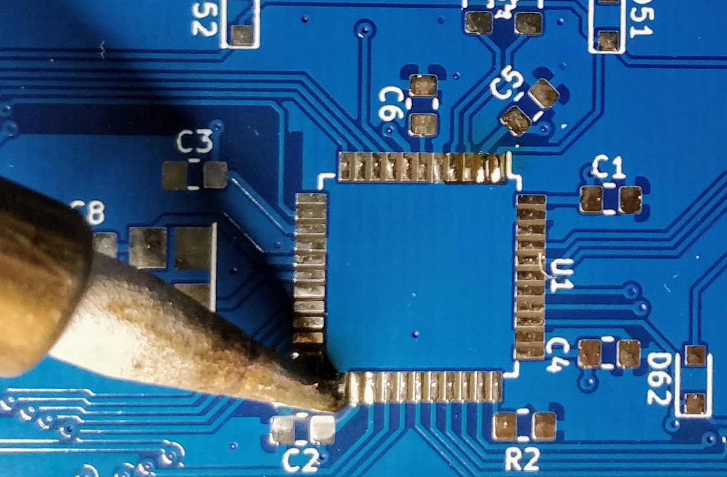
What’s cooking next

That’s all for today (it took so long to write this). In the next episode I’ll try to cover:

  • producing manufacturing files and sending them to the manufacturer
  • selecting the right components
  • SMT soldering thechniques with a regular soldering iron
  • creating the firmware
  • testing the PCB

Thanks for following!
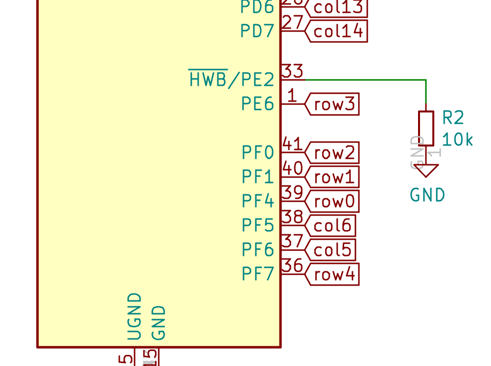
Designing a keyboard from scratch - Part 2

28 minute read

Updates

  • I fixed the passive components footprints to be 0805 instead of 1206, based on a previous design I made. Those are still easy to hand-solder, but leave more empty space around the MCU to route signals.
  • The MCU placement and matrix connection schema is now correct. I forgot that it will be under the PCB and thus everything is mirrored.
  • Thanks to Druz who discovered there was a mismatch between the reset button in the electronic schema and the footprint

Preamble

Welcome for the second episode of this series of post about designing a full fledged keyboard from scratch. The first episode focused on the electronic schema of the keyboard controller. This episode will cover the following topics:

  • how to design the matrix electronic schema
  • how to assign references and values to its components
  • the first steps of the PCB layout

The matrix

Trust me, it will be probably the most boring part of this series. I’m going to design the electronic schema of 67 switches and diodes.

Since the MCU schema is taking some space in the main sheet, I recommend creating a hierarchical sheet to place the matrix components. This can be done by pressing the s shortcut and clicking anywhere in the schema. The following window should open:

Hierarchical sheet

Because I’m designing the matrix, I named this new sheet matrix (yes that’s quite original). It is possible to access this hierarchical sheet with the ViewShow Hierarchical Navigator menu:

Hierarchical navigator

Clicking on the matrix will open this new (blank) schema sheet.

Let’s build the matrix now. As I explained in the previous article, the matrix is the combination of one switch and one diode per key. It’s cumbersome to add those components by hand for all the 67 keys, so I’m going to explain how to do it with a selection copy. There are other ways to do it, for instance by generating the schema with this tool or this other tool.

Let’s first design our key cell, by adding a SW_PUSH and a regular D diode. Next wire them as in this schema (notice that there’s no connection between the vertical and horizontal wire):

Matrix cell

This cell forms the atomic core of the matrix. Once done (if you also are following this for your design make sure the wires have the same size as mine), maintain the shift key depressed and drag a selection around the cell (wire included). This will duplicate the selection (our cell), then move the mouse pointer so that the diode bottom pin is perfectly aligned with the first cell horizontal wire:

Drag copy cell

Then click the left mouse button to validate. Now repeat the shift drag selection operation on both cells at once to duplicate them and form a 4 keys schema:

Drag copy cell x2

Note that it is also possible to perform the move and place with the keyboard arrow keys and enter to validate.

Next, repeat the same with the 4 cells to form a line of 8, then a line of 16 cells, and remove the last one to form a 15 keys row. If the key rows is larger than the page, you can increase the sheet size by going to FilePage Settings and change the Paper Size to A3.

This should look like this:

Matrix one row

Let’s add a label to the row (Ctrl-H):

Matrix one row

Let’s now do the other rows. I’m going to apply the same technique, just do a shift drag selection around the whole row0 and move it downward so that the wires of the columns connect:

Matrix second row

And do the same for the next 3 rows, this will give this nice array of switches:

Matrix all rows

Note that I have pruned the extra vertical wires of the last row with a large regular selection and pressing the del key. It is also possible to do the same for the right extra wires on all rows.

Next, edit all the row labels to make them row1, row2, etc. The columns also needs to be labelled. Start by adding a global label on the first column and label it col0. Use the shift-select trick to create a second one, then 2 extra ones, then 4 etc until all the columns are labelled. Edit the labels so that they are labelled from col0 to col14.

Matrix labelled

Finally that was quick! But I suspect you’ve noticed there are too many keys in this matrix. I’m going to remove some of the extraneous switches so that the wiring would look like this if laid out on the physical layout:

Matrix wiring

To eliminate the unneeded cells it’s as easy as selecting their switch and diode (and as less wire as possible) with a drag selection and pressing the del key.

The matrix should now look like this:

Matrix wiring 67 keys

Now, I’m going to reference all the switches and diodes I just placed. Since I’m quite lazy, I’ll use the automatic referencing feature. If you want to reference switches by coordinates (ie first switch is K000, second one K001, but first of row1 is K100, etc), you’ll have to perform that manually (or write a script to directly modify the .sch file, or edit it with a text editor). I will just use increasing numbers in line.

Use the ToolsAnnotate Schematics to open the annotation window:

Annotation of the matrix

Make sure to annotate only the current page, and to Sort components by Y position. Once done, the matrix diodes and switches will have a proper unique reference identifiers. If you somehow failed, the same dialog can also erase all references (trust me, it’s easy to make a mistake, like for instance applying references to the whole schematics and not only to the current sheet).

The next step is to label each switches with their key character or name (ie K1 will be GRV, K2 #1, K17 Q, etc). This will help when laying out the PCB, because the key name will be visible, compared to referring keys only by their identifier. I could have use the key name as the identifier (for instance K_SPACE, or K_ENTER), but Kicad wants each reference to contain a number which makes things look ugly in the end.

To assign key names to the switches, I’m going to use the ToolsEdit Symbol Fields window. This opens a new dialog that allows to group components by reference or value (or both) and to edit component values all at once:

Editing Symbol Fields

Open the K1-K67 group, and start assigning the correct key names in the value column to the switches in order:

Editing Key Values

Once done, the matrix itself shouldn’t be different than it was before. The key names don’t appear, because the KEYSW symbol have the value marked as invisible. Unfortunately it isn’t possible to edit this symbol with the Symbol Editor, toggle the value visibility and reassign the symbol to all the KEYSW in the matrix. Kicad allows you to do that, but doesn’t change the visibility of the existing symbols. If I want the key name to appear I will have to edit manually all the 67 switches to turn on their value visibility or edit the matrix.sch file with a text editor. I chose to alter the matrix.sch file with the sed command. Make sure to save the schema, close it and git commit the file and project before doing this:

sed -i -r -e 's/^F 1 "([^ ]+)" H ([0-9]+) ([0-9]+) ([0-9]+)  0001 C CNN/F 1 "\1" H \2 \3 \4  0000 C CNN/' matrix.sch

Reopen the root schema, then the matrix and you should see something like this:

Showing key names

The matrix is now finished. The perfectionist among us could move the key values or diode references so that they don’t collide (but remember I’m lazy).

The next step is to finish the main schema.

Prepare the MCU schema

Using the ToolsAnnotate Symbols, I’m going to assign references to the main sheet (and only this one). Once done, to ease laying out the MCU on the PCB, I’m going to tentatively assign rows and columns to the Atmega32U4 pins.

To do that, I need to tell you a few rules about laying out our board:

  • the D+/D- signal form a differential pair. They need to be traced as directly as possible.
  • there’s only limited space available on the board between switches to put the MCU. Except behind the space bar where there’s no switch at all.
  • the connections between the MCU and the matrix should cross each others as little as possible, thus the MCU should be oriented wisely so that left columns are assigned to pins to the left of the MCU and reverse.

The physical layout of the MCU looks like this (it’s called a pinout):

Showing key names

With this in mind, if I want to minimize the length of the D+/D- paths, and considering that the MCU will stay behind the space bar at the bottom of the PCB and the USB port at the top, I will have to put the D+/D- pads face up. With this orientation, this means that:

  • PF0, PF1, PF4, PF5, PF6, PF7 will be on the right
  • PD0, PD1, PD2, PD3, PD5 will be on the left
  • PD4, PD6, PD7 on the bottom left
  • PB5, PB6, PC6, PC7 on the bottom right

Since the MCU will be on the back of the PCB, when looking from the top, then it is possible to assign col0 to col4 to bottom right pads (which will be left as seen from the bottom), col5 to col6 to the right pads, col8 to col14 to the bottom left corner. The rows can be connected on the PFx pins on the right.

Of course this is an attempt that will serve as a guide during the PCB layout. There are great chances that I’ll have to come back to the schema to reassign columns or rows to the MCU pins as I see fit.

Here’s the schema with the rows and columns connected:

Wired Atmega32U4

Check for errors

Before moving forward, I need to make sure everything is connected correctly. Kicad contains a tool called the Electrical Rules Checker that can help debug the schema connectivity. It is available in the Inspect menu.

The ERC shouldn’t display any error except a few about missing power. The ERC is complaining that our power nets (+5V, Vcc and GND) are not connected to real power sources. In fact all come out of the USB connector, but Kicad doesn’t know that this connector provides a source of power (or ground).

Hopefully there’s a way in Kicad to artificially tell those symbols are connected to a real power source. Those sources need to be connected to the special PWR_FLAG power symbol. Press the q shortcut to place a power symbol, and search for PWR_FLAG:

PWR_FLAG to the rescue

Place it on a wire connecting to GND, then place another one for Vcc and +5V:

PWR_FLAG to the rescue

With those PWR_FLAG symbols in place, the ERC doesn’t report any errors anymore. I’m relatively confident the schema is right, but I suggest, if you also design a keyboard to double-check (and even triple-check) or ask someone in the community to check it for you (you wouldn’t want to receive a PCB that has a design flaw and that doesn’t work.)

Footprints

Up until now I’ve only talked about the electronic symbols. Serious things are still ahead. In this step, I’m going to assign footprints to the components of our electronic schema. A component footprint is a physical layout describing how the component will be soldered on the PCB (that’s actually a bit more than that). For instance, for a normal through-hole resistor, the footprint will have 2 holes surrounded by soldering pads spaced at a normalized distance, the same for IC or SMD components.

This project will only have SMD components (because they are much smaller). SMD components are soldered directly on the PCB. On the other hand I want to be able to solder them with my usual soldering iron and not a reflow oven or an hot-air gun. That means I have to choose SMD components that are big enough to be able to do that easily.

For passive components like resistors, capacitors, etc, there are several normalized sizes. From bigger ones like 1206, 0805, 0603, 0402, or even 0201. In fact this number represents the size of the component in inches (centi-inches even), so for instance 1206 means a length of 0.12 inch and a width of 0.6 inch (which makes them the large). It is relatively easy to hand-solder 1206 and 0805 components with a regular iron solder (I’ll explain the techniques in a subsequent post), but not so much for the smaller ones. Soldering such components requires a magnifying glass, a pair of tweezers and soldering flux at the very least.

Here’s the exact size of those different components:

SMT sizes, based on original by Zureks

For this PCB, I’m going to choose the 0805 (and not 1206 as I originally wrote) size so that it’s still easy to solder the components but allows routing traces around the MCU. Other components have different packages of different size too. For instances, diodes exists in SOD323, SOD123, MiniMelf packages etc. SOD123 packages are much easier to solder than MiniMELF packages, because MELF components are cylindrical (and they tend to roll or misalign easily).

Let’s assign footprints to the components now. Go to the Tools menu and choose Assign footprints:

Assign footprints

This dialog shows on the left column all the component classes, on the middle our components and on the right the individual footprints.

The task is to assign a given footprint to the references. With this, we can assign footprints in bulk, but it is also possible to assign a footprint to a given component directly from the schema by editing it (shortcut e).

As said earlier, let’s assign a 0805 footprint to our capacitors. Select all C references at once, select the Capacitor_SMD class in the left column, and select the Capacitor_SMD:C_0805_2012Metric_Pad1.15x1.40mm_HandSolder footprint. I specifically chose the HandSolder variant, because the pads are a bit larger than a regular 0805 (in fact you can almost place a 0805 component in one pad of such footprint).

Assign capacitors footprint

Do the same for the other components, and assign (use the search function to find the specific parts):

Component Footprint Comment
Diodes Diode_SMD:D_SOD-123  
500mA Fuse Fuse:Fuse_1206_3216Metric_Pad1.42x1.75mm_HandSolder  
ISP header random-keyboard-parts:Reset_Pretty-Mask  
K?? switches Alps_Only:ALPS-1U we’ll come back later to this
Capacitors Capacitor_SMD:C_0805_2012Metric_Pad1.15x1.40mm_HandSolder  
Resistors Resistor_SMD:R_0805_2012Metric_Pad1.15x1.40mm_HandSolder  
Atmega32U4 Package_QFP:TQFP-44_10x10mm_P0.8mm it should already be assigned, but just in case
Reset push button Button_Switch_SMD:SW_SPST_SKQG_WithStem  
PRTR5V0U2X random-keyboard-parts:SOT143B  
USB Type-C connector Type-C:HRO-TYPE-C-31-M-12-HandSoldering  
Crystal Crystal:Crystal_SMD_3225-4Pin_3.2x2.5mm_HandSoldering  

As an astute reader you might have noticed that I assigned 1U variants to all our switches, but that the library contained all the standard key sizes. Ai03 library contains footprints for the exact size of the various keys available on a keyboard which greatly simplifies laying out the switch footprints on the PCB. For the MX variants, larger keys also contains the PCB holes for the stabilizers. Because the references I attributed to the switches don’t tell which key it is, it’s relatively hard to assign the correct key size footprint directly from the Assign footprints dialog box. Instead I’m going to edit the handful keys larger than 1U directly from the schema, by pressing e on the switch symbol and assigning the following footprints:

Key Footprint
TAB Alps_Only:ALPS-1.5U
CapsLock Alps_Only:ALPS-1.75U
LShift Alps_Only:ALPS-2.25U
LCtrl Alps_Only:ALPS-1.5U
LAlt Alps_Only:ALPS-1.25U
LCommand Alps_Only:ALPS-1.5U
Space Alps_Only:ALPS-6.5U
RAlt Alps_Only:ALPS-1.25U
RShift Alps_Only:ALPS-1.75U
Enter Alps_Only:ALPS-2.25U
Backspace Alps_Only:ALPS-2U
\| Alps_Only:ALPS-1.5U

To double-check, reopen the Assign footprints dialog box and make sure everything has a footprint.

PCB Preparation

The schema is now ready to be laid out on the PCB. The rest of the work will happen in the PCB layout program that is called pcbnew in Kicad. You can start it from the schema editor by clicking on the PCB icon in the toolbar.

This will open the PCB editor with a blank view and grid. Do what ai03 suggests in his guide to setup the user grids: create a user grid settings with X: 0.79375 mm and Y: 0.79375 mm (make sure to be in mm, refer to ai03’s guide for the complete instructions):

PCB Grid Settings

Copper tracks have resistance. This means that a track has a voltage drop, power dissipation, and a temperature rise when current flows through it. The resistance is a function of the track length, width, thickness and of course resistivity of its material.

For signal tracks (like the matrix), there’s very few current involved, we can keep the Kicad default (0.25 mm or a bit less than 10 mils). The usual advice is to make the tracks as large as the design allows. A keyboard by definition has a large PCB. Since there’s no led nor any features other than the switches and the electronic components, this PCB will be reasonably empty. It’s a good news: we can make the power tracks as large as we need. By power tracks I mean in fact the +5V, VCC but also GND. In fact, GND is as important as the other power signals because it will carry all the return currents from the ICs, and thus is subject to as much current as the other power nets.

So power tracks are required to be larger, but what size do we have to use? Ai03 in his guide suggests 15 mils. This sounds right, but in fact there is a way to compute the exact track width. Unfortunately determining trace width is a complex science. The IPC has published a (paying) standard, IPC-2152. IPC-2152 publishes an abacus that allows to find the trace width based on projected current, copper thickness and temperature rise. Hopefully we can also use one of the numerous PCB trace width calculator.
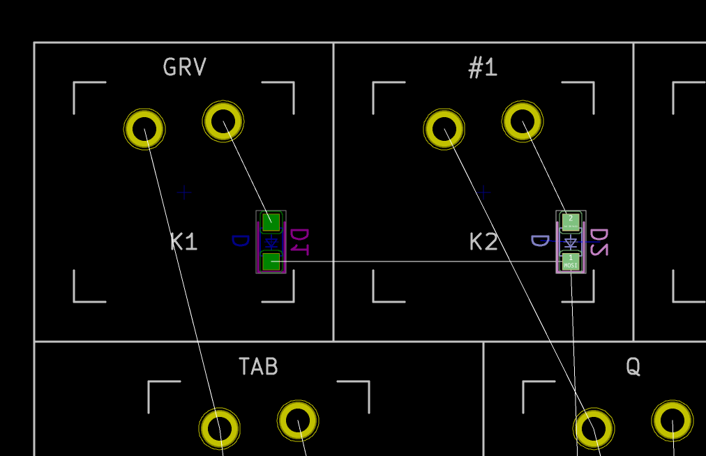
Copper thickness on PCB is measured in oz/ft2 (looks like the metric system lost again). The default is usually 1 oz/ft2. If we have 500mA, default 1oz/ft2, and a maximum temperature rise of 5ºC (we don’t want the temperature to increase too much), the calculator returns 7.1 mils in open air, or 18 mils for inner layer trace. The IPC-2152 standards does it’s calculation with tracks spaced by 1 inch. This isn’t really practical for a real life PCB, so we might just want to aim for a smaller temperature rise (two parallel tracks at 500mA will increase temperature more than only one) to 2ºC (another solution could be to increase the projected current as if we had more current in one track simulating two close tracks). The result is a trace width of 12 mils.
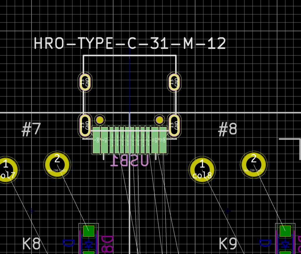
Of course nothing is perfect, and the copper traces might contain debris or be etched. Any of those modifications will increase the trace resistance, and thus the temperature rise. Because this keyboard will be in a closed unventilated case, we need to limit the temperature rise as much as we can afford (remember that the MCU will also produce heat). Because of that, I’m going to add a safe margin and use 15 mils (as ai03 suggested) for the power traces.

Doing the same reasoning in reverse we could also reduce the size of the signal traces. Most manufacturer nowadays can do 5 mils (0.127 mm) traces. We have plenty of space on this keyboard PCB, and it costs the exact same thing if we do 5 mils traces or 10 mils traces, so let’s keep the default 10 mils.

Kicad has a feature that allows you to declare trace width based on the net they’re built for (ie connections between components). This allows to automatically adapt the trace width depending on if the route is for power or signal. This can be done in the FileBoard Setup dialog box, section Design RulesNet classes.

Click on the + sign to add a class called Power, and adjust trace width to 15 mils (you have to be in inches mode to do that). Then in the bottom part of the dialog box, assign this power class to the VCC, +5V and GND nets:

Assign classes to net

Finally, let’s import the components to the PCB by going to ToolsUpdate PCB from schematics…. This gives this pile of components:

Importing components in the PCB

You might notice all the components have been packed together (all the keys, all the diodes, etc). If you zoom in on the components, you’ll notice that their pads are all drawn in red. This means those components are laid on the top of the PCB. This is the perfect time to talk about PCB layers.

A PCB is a dielectric board usually made from FR4 fiberglass. Copper planes are sandwiching this board, on which the traces are drawn. There can be one layer, 2 layers (one at the top, one at the bottom), 4 layers (2 on top separated by a dielectric substrate, and 2 at the bottom), 6 layers, etc. Each couple of layers increases the manufacturing price. For this keyboard, a 2 layers PCB will be enough.

Kicad defaults to two layers boards (you can add more if needed), one on top (the red one) and one on the bottom (the green one), they are respectively named: F.Cu (Front copper), and B.Cu (back copper). But Kicad also defines other layers:

Kicad Layers

Here is a table summarizing their usages:

Layer name Type Usage
Cu Technical pair Copper layer for traces
Adhes Technical pair application of adhesive to stick SMD components to the board prior to soldering
Paste Technical pair mask to place solder paste for reflow soldering
SilkS Technical pair where the components are drawn
Mask Technical pair defines the areas free of soldermask like component pads
CrtYd Technical pair show how much space a component physically takes
Fab Technical pair documentation for manufacturing
Edge.cuts Independent the board shape
Margin Independent to define a safe margin for edge cuts
Dwgs Optional can be used for instructions, drawings. Some footprints use them
Cmts Optional can be used for instructions, drawings. Some footprints use them
ECO1/2 Optional user specific, never used in footprints

Since this PCB will have two layers, it would be possible to evenly spread the components on both layers. Since there are much more room on the back (all the switches take space on the top), it’s preferable to put all the SMD components on the back (bottom layer). Also, putting all the components on the same layer would reduce the manufacturing costs if I wanted to order soldering. Note that this will also reduce the number of vias (a via is a hole in the PCB that connects electrically two layers).

First let’s move all SMD component footprints to the B.Cu layer. To do that drag select the components and press the f shortcut (to flip them to the other face). If they get placed on the way or far away, press m to move them closer.

Flipped PCB components

Laying out components

The most difficult task in designing a PCB is routing the copper traces between components. Those traces should be carefully designed to prevent EMI (I’ll talk about that in a subsequent post), not cross layers too many times etc. Routing is an iterative process that is very time consuming, and can be considered as an art (at which I’m a newbie, you’ll see that soon). But before we can start routing the PCB, we need to place the components. Laying out the component is more than half of the routing work. Components badly placed can make routing hard or impossible.

Some components can’t be placed anywhere, think for instance of the switches that need to be placed where the keys will be. Same for the USB-C connector. Then other components might have constraints that also mandate where they are, for instance the decoupling capacitors that need to be close to the MCU to be effective.

Placing the switches

I’m going to start with the key switches because that’s them that will define the size and aspect of the PCB. Let’s switch to the User Grid 0.7937 mm which has been designed to place switches. This grid is 1/24th of a key. The task is to move every switch footprint in the order of the layout of the final keyboard, starting with the GRV key. With this User Grid in place, the switches will snap together perfectly. It is also possible to use the arrow keys to move the components in place.

Aligning keys

Keep going until all the keys form the layout. Note that the key name (which we put in the component value earlier) appears on the footprint. This simplifies the placement of the switches.

If you struggle to find a key, you can use the Find functionality (Ctrl-F) and enter the key reference. Even better use the t shortcut to activate the Get & Move Footprint feature, enter the reference, then move it to the right place.

Here again it is easy since we’re laying out the keys in order of increasing K? reference (from K1 to K67). Make sure all switches outer white bounds are aligned when placing a new key next to an already placed one. Their borders should only form one thin white line. It might be easier to hide the rats-nest while placing the switches (there’s a button in the left vertical toolbar to do that).

In no time you’ll get the whole matrix properly aligned:

All matrix aligned

In the process of aligning the keys, I noticed that I misattributed the footprints of two keys. To correct such mistake, you need to go back to the schema, change the footprints to the correct ones (by editing the components). Next go back to the PCB editor and click on the ToolsUpdate PCB from schematics…. In this dialog box, make sure to select the Update footprints and the Reassociate footprints by reference method. The misattributed footprints should be corrected automatically.

Placing the diodes

The next step is also quite tedious. It consists of moving all the diodes to their parent switch positions (by using the t shortcut). Still with the switch User Grid, start with D1, move it to the K1 position, rotate it as you see fit with the r shortcut. Do the same for D2 and so on:

Placing diodes

It’s best to do this part with the rats-nest visible. The rats-nest is the forest of white lines that connect all pads part of the same net. It’s a visual help used during trace routing. In the diode layout phase it also helps visualize rows and columns. For instance in the picture above, D1 pad 1 and D2 pad 2 are connected to form a row.

Once done, the result looks like that (the entropy has greatly declined !):

All diodes placed

USB-C Connector

The next components to lay out is the USB Type-C connector and its associated components (like the fuse, the ESD protection IC, etc).

There are different schools regarding where to place the USB connector. I find centered connector to be more appealing visually. Still with the switch User Grid settings, move the connector to the center top of the board (which happen to be between the 7 and 8 key):

USB-C connector

Since the footprints hotpoint is exactly at the center, and thanks to the switch User Grid Settings, it is easy to perfectly snap in the connector between two keys.

Next, we’ll move the components that needs to be close to the USB connector there. It means both 5.1k resistors, the PTC fuse and the ESD protection device. Notice how I carefully placed those to minimize the number of nets crossing:

USB-C components

The MCU

Now, I need to take care of the MCU and the components that are connected to it. The MCU is quite large, but hopefully there is enough room between the space key switch and the other switches. Ideally we have to route the D+/D- differential pair with the shortest path possible (to control the USB data-lines impedance). The crystal also needs some room. It looks like the best way is to orient the MCU with the D+/D- pins face up and the crystal to it’s right. Of course, things will probably change when I’ll start routing:

MCU tentative layout

Around the MCU, there are so many nets that it might be hard to see what’s connected to what. At any time it is possible to highlight a net by using the Highlight net function (shortcut \`). For instance to better see the nets around the crystal:

MCU net highlight

The crystal needs to be connected to the two 22pF capacitors and the two XTAL1 and XTAL2 pads on the MCU. The following arrangement allows to take advantage of the free space around the MCU while minimizing the number of crossing nets and leaving room for routing the matrix around:

MCU Crystal laid out

The D+/D- differential pair (the USB data lines) requires two 22 ohms resistors to make sure the USB bus is terminated with the correct impedance. Those have to be placed as close as possible to the MCU. We can orient them in the direction of the USB-C connector:

USB data line impedance

The next step is to add a decoupling capacitor for each VCC pad of the MCU. We’ll keep the 10uF capacitor close to UVCC and VBUS as I explained in the first part. The rest of the 0.1uF capacitors will be moved close to the other VCC pins. The idea again is to minimize the number of nets crossing while still leaving room for routing traces. We also do the same for the RESET pull-up resistor, the UCAP capacitor and the HWB resistor, and finally the reset push button:

MCU Capacitors

As said earlier, this is a tentative layout. When I’ll start the routing, there are very good chances that I’ll have to move things a little. Note also that I haven’t placed the ISP header. I’ll do that during routing, because the matrix might not be hooked exactly like we did above in the end, and I might reuse the MISO, MOSI or SCK pins for the matrix.

The board now looks like this:

PCB laid out

Notice that all components are now placed inside the switch footprints, thanks to the SMD components small size.

Cutting edges

Now that everything is approximately at the right place, we can design the PCB border. In order to do that, I’m going to draw the contour while being in the Edge.Cuts layer. This will let the manufacturer know where the board should be cut. This can be used to give specific forms to the PCB. In this case, I’m going to draw the border exactly on the key bounding boxes, including the USB connector. The HRO-TYPE-C-31-M-12 connector has four through-hole pins that needs to be soldered which means the PCB must extend under those (this will help secure the connector and prevent it to become lose while connecting/disconnecting cables frequently).

Let’s start at the top-right corner (any corner will work though), select the Edge.Cuts layer and the Arc tool. Switch to the switch User Grid settings if you’re not in it and click in the middle of the top right corner:

Top Right Edge Cut

Select the arc that just has been drawn and Copy it (Ctrl-C) by clicking on its control points. Then paste the copy (Ctrl-V) and move it to the bottom-right corner (or any other corner). Rotate it by pressing r until it has the correct orientation and place it in the corner:

Bottom left Edge Cut

Repeat for the two remaining corners. Before adding the edge lines, I believe it’s easier to prepare the USB connector. Draw an Arc on the left part of the connector and continue it with a line:

Left USB cut

Then the draw the horizontal and right vertical edge:

Right USB cut

And finally copy the left arc (make sure to click the the bottom left control point):

Copy Left USB cut

Next, move the arc to the right part of the usb and rotate it (r):

Paste at right USB cut

Then finish the border by drawing Lines connecting all the rounded corners:

Paste at right USB cut

Now, inspect visually the edge cuts to make sure everything is aligned and connected. To have a better view, I recommend to hide the Dwgs.User layer (where the switches bounding boxes are drawn). I also ran the Design Rule Checker (from the Tools menu) to spot any edge cut errors:

DRC Edge Cuts hole error

In this case the line was extending into the arc too much (by one grid step). It was easy to fix but couldn’t be found except with the DRC.

The big picture

If you followed the design so far, you should have the following PCB:

The big picture

3D Visualization

There’s a feature in the Kicad PCB editor to see the PCB in 3D. I don’t have the tracks laid out yet, but all the components have been placed so there’s something to see. Activate View3D Viewer to see the board top. You can rotate the board (not the best virtual ball I’ve ever used) with the mouse and see the bottom face (which contains our components). You’ll soon discover that there’s no 3D model for the USB Type-C connector. Hopefully it’s easy to add it. First edit the USB Type-C connector, then click on the Footprint Properties icon and finally click on the 3D Settings tab:

No Type-C 3D Model

Kicad doesn’t know where to load the USB Type-C connector 3D model, click on the folder icon to add it and chose the Type-C.pretty/HRO TYPE-C-31-M-12.step file:

Load the Type C

This loads the 3D model but in a completely off orientation:

Bad orientation

Apply the following transformation so that the connector has the correct orientation:

Type-C Correct Orientation

Save the footprint, and finally the board can be rendered with all the components:

AEK67 PCB 3D View

What’s cooking next

That’s all for today. We’re still far from having a working PCB, and in the next episode I’ll cover:

  • routing the traces
  • power ground pour
  • adding drawings on the silkscreen
  • manufacturing the PCB

Thanks for following!

Want to read the next part? Then click here for the Designing a Keyboard part 3